.avif)

Executive Summary
· Metamaterials are artificial structures not typically found in nature that can be designed to have special properties. These structures can be customized to bend, absorb, or scatter waves including light, radio wave, sound, and seismic. They also range from nano to meter scale in specific ways for specific functions.
· Metamaterials are most used in semiconductors, opto-electronics, consumer electronics such as cellphone cameras, and telecommunications. Research activity is spiking around the use of metamaterials in security and surveillance technology, as well as healthcare applications like diagnostic imaging.
· The applications of metamaterials play a role in the materials used to construct them. For example, photonics and optical applications use metals, oxides, and semiconductor materials, which have strong optical responses. Acoustic and thermal applications use elastomers and rubber materials that can bend and deform.
· 2D metasurfaces, in which the engineered functionality is concentrated on a surface, are most common in the research landscape, but 3D and 1D metamaterials are used in specialized applications.
For decades, metamaterials, artificial structures with properties not readily found in natural materials were a physicist's curiosity. These structural materials can have numerous extraordinary properties, including the ability to bend light backward, make objects “invisible”, or channel sound in unprecedented ways. Today, these novelties are turning into commercial opportunities.
Three forces have converged to bring these materials out of the realm of science fiction and into commercial usage. First, nanofabrication techniques now enable cost-effective production of subwavelength structures. Second, AI-driven inverse design and topology optimization have compressed development cycles significantly. Lastly, strong demand from 6G communications, wearable sensors, AR/VR displays, and quantum photonics is creating markets large enough to justify the manufacturing investment.
Which industries are starting to utilize metamaterials? What applications are they being used for, and which materials are receiving the most attention from researchers? As this field transitions from laboratory demonstrations to engineered products, it’s important to understand where market demand is growing and how these innovative materials will transform defense, aerospace, consumer electronics, and more.
Note: Since a document may describe more than one chemistry or material or application, classifications in this analysis are not mutually exclusive and category totals do not sum to 100%.
Publication trends reveal global growth of metamaterials
We analyzed the CAS Content CollectionTM, the largest human-curated repository of scientific information, to better understand where the field of metamaterials is headed. We found that publication activity has expanded dramatically over the past decade, reflecting growing scientific interest and commercial relevance (see Figure 1A).
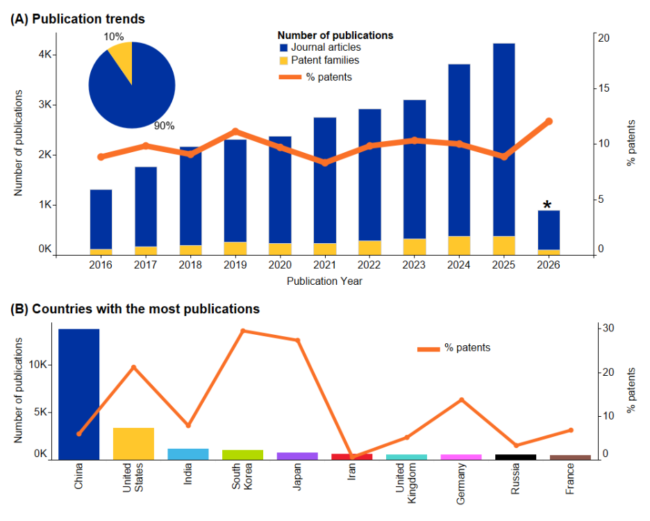
Scientific output has grown rapidly, but patent activity has also kept pace, with filings more than tripling between 2016 and 2025, consistently accounting for about 10% of annual publications. This combination of expanding research output and strong IP activity is evidence that many metamaterial advances are now viewed as scientific discoveries and technologies with tangible commercial value.
Patent activity varies substantially by country, revealing different innovation strategies (see Figure 1B). Although China leads in publication volume, South Korea, Japan, the United States, and Germany show substantially higher patent-to-publication ratios. These patterns suggest that leadership in metamaterials may depend not only on research output but also on the ability to convert discoveries into protected technologies and commercial products.
The patent trends in Figure 1 were analyzed using CAS SciFinder®, which aggregates chemistry and related science data from global sources. Researchers exploring similar trends can access AI-enabled search capabilities to identify patterns in their specific research areas.
Why now for metamaterials?
Three forces converge: nanofabrication techniques, AI-driven inverse design and topology optimization, and strong demand.
Metamaterial applications in consumer electronics, stealth technology, and more
Metamaterials have outstanding industrial potential because their sub-wavelength architecture lets them manipulate waves such as electromagnetic, acoustic, and mechanical, in ways natural materials cannot. They contain engineered unit-cells smaller than the target wavelength which produce desired effects. Because the waves they control scale from nanometers to meters, metamaterials find applications in many sectors such as telecommunications, imaging and sensing, medical diagnostics, defense, and noise control.
Our analysis of publications across industries shows that consumer electronics, imaging and display technologies, semiconductors and optoelectronics, and telecommunications dominate research output (see Figure 2).
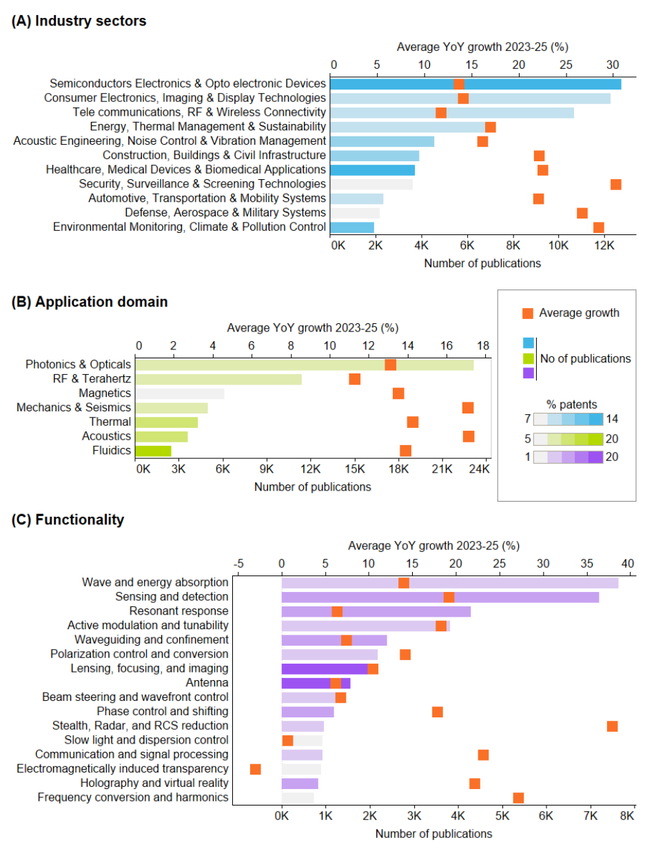
The application landscape in Figure 2B reinforces these findings. Photonics & opticals accounts for over four-fifths of all publications, reflecting the maturity of optical metamaterials and the enormous commercial pull from the consumer electronics, telecommunications, and semiconductor industries. Yet, this dominance masks a critical insight: radio frequency (RF) and terahertz applications show the second-highest concentration, consistent with strong interest in wireless connectivity, radar, sensing, 5G/6G infrastructure, and high-frequency communication systems. The overlap between these domains is not coincidental, as many metamaterial innovations serve dual purposes across optical and RF applications.
The growth trajectories within these sectors reveal where momentum is building. As seen in Figure 2A, security, surveillance & screening technologies show the highest year-over-year (YoY) growth, followed closely by defense & aerospace and environmental monitoring. Notably, the most established sectors, consumer electronics and semiconductors, show more modest but steady growth. This pattern is consistent with maturation rather than saturation; engineering advances such as electromagnetic-control capabilities that were once concentrated in the defense sector seem to be adapted for commercial platforms while optimizing scalability and cost.
Our functionality analysis shows a clear hierarchy of commercial readiness intersecting strategically with industry demands (see Figure 2C). Wave and energy absorption are the most-researched functions, which underscores metamaterials’ value as absorbers for electromagnetic interference control and thermal management. Similarly, lensing, focusing, and imaging functions and antenna functionality have the greatest concentration of patent activity. The YoY growth of stealth, radar, and RCS reduction functions stands out, however, and it reiterates the growing market in security, surveillance & screening technologies that we found in the industry sector analysis in Figure 2A.
Functionality co-occurrence analysis reveals innovative uses for metamaterials
We analyzed the co-occurrence of functionality and industry sectors to understand how metamaterials are being used today (see Figure 3). As noted, wave absorption applications dominate research output, showing remarkably uniform distribution across consumer electronics, semiconductors, and telecommunications. This universality reflects absorption’s foundational role in metamaterials. Sectors grappling with electromagnetic interference, unwanted reflections, or radar signatures can benefit from metamaterial absorbers where compactness, selectivity, or multifunctionality is required.
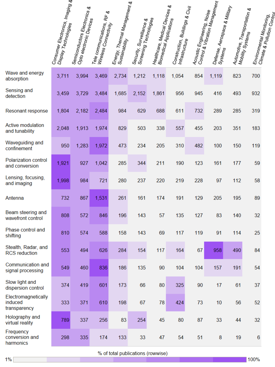
Sensing and detection applications constitute the second major concentration, with strong growth trajectories and elevated patent activity relative to publication share. However, sensing shows strategic concentration rather than uniform distribution, clustering heavily in security & surveillance, healthcare, and environmental monitoring. This pattern indicates sector-specific optimization: healthcare emphasizes biosensing and diagnostic imaging; environmental monitoring focuses on pollutant and climate sensors; and security prioritizes threat detection and screening technologies.
The most revealing patterns emerge in specialized functionalities showing sharp industry concentration. Antenna applications, despite modest overall publication volume, command the highest patent percentage of any functionality and concentrate heavily in telecommunications, which shows exceptional focus on antenna, waveguiding, and signal processing. This specialization reflects infrastructure priorities, such as directing, transmitting, and processing electromagnetic signals across specific frequency bands.
Stealth and radar cross-section reduction also demonstrates strong specialization, appearing in the defense & aerospace and automotive sectors, where these capabilities most clearly justify higher development costs. Similarly, holography and virtual reality applications cluster overwhelmingly in consumer electronics while barely registering elsewhere, reflecting that industry’s drive toward immersive displays.
Active modulation and tunability functionalities show balanced representation across consumer electronics, semiconductors, and telecommunications. Dynamic reconfiguration of metamaterial properties enables adaptive optics in cameras, tunable filters in spectrum analyzers, and reconfigurable antennas in wireless systems, demonstrating how a single technical capability can generate diverse applications as it matures.
At the commercial frontier, lensing and imaging applications show strong patent activity driven by smartphone manufacturers seeking thinner optical systems and AR/VR developers requiring compact displays. At the opposite extreme, electromagnetically induced transparency and slow light applications show minimal patent percentages and, in some cases, negative growth.
Ask complex, multi-part questions and receive context-based, cited answers sourced from 150+ years of curated and human-verified science.
Material choices coincide with applications
While application trends reveal where market demand is emerging, the materials landscape reveals the legacy of metamaterials' plasmonic origins and the diversification necessary for commercial viability. When we examined which materials are leading in research publications, we found that metals & plasmonic conductors dominate, reflecting the continuing importance of conductive structures in optical, RF, and terahertz regimes (see Figure 4A).
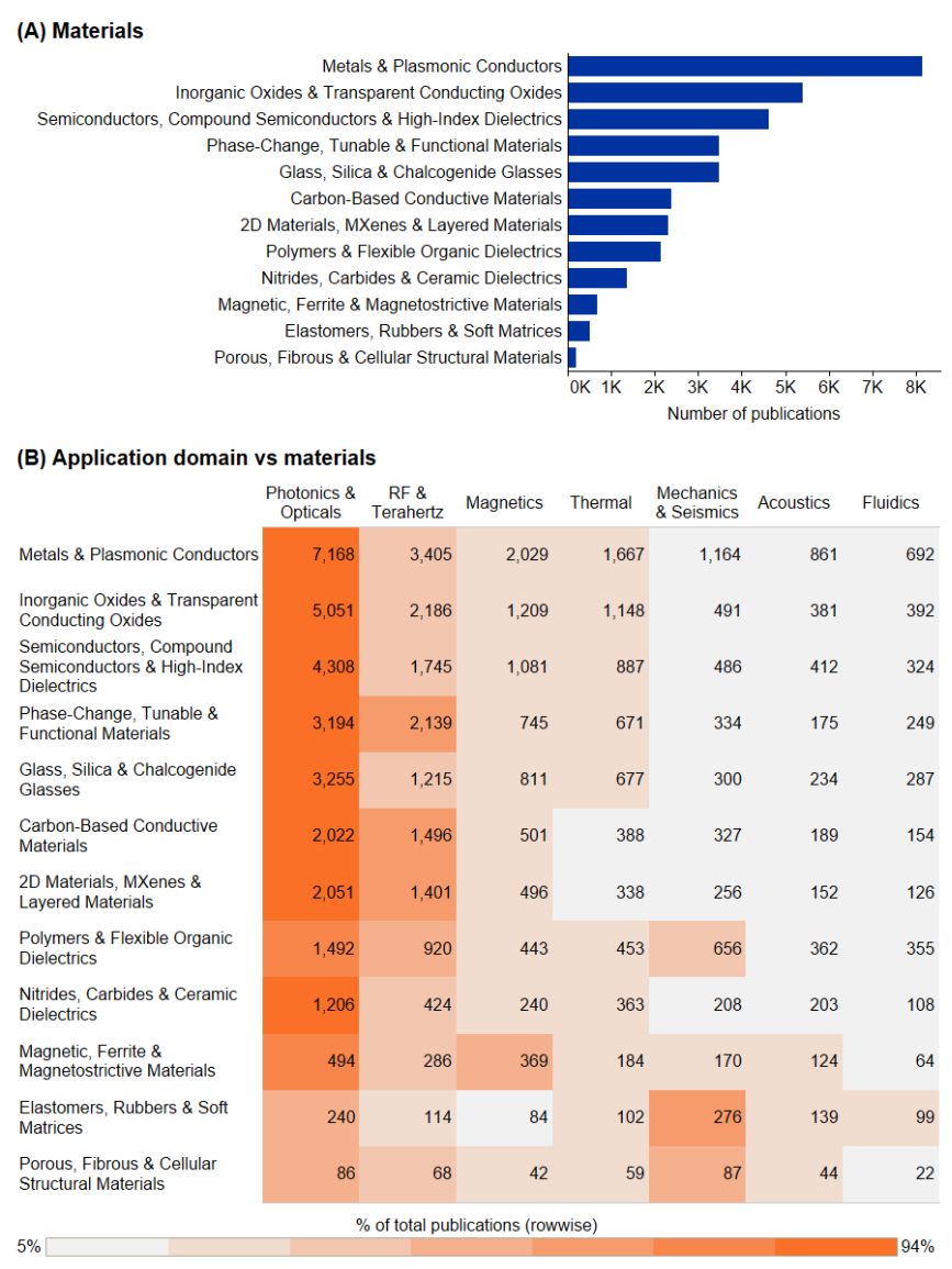
Inorganic oxides & transparent conducting oxides show strong representation, particularly in photonic applications where transparency and electrical conductivity must coexist. Certain transparent conducting oxides enable active metamaterial devices where optical properties change in response to electrical signals, an essential capability for displays, smart windows, and adaptive optics.
Semiconductors, compound semiconductors & high-index dielectrics represent the third-largest material category, reflecting the drive toward CMOS-compatible metamaterials that can integrate with existing semiconductor manufacturing. This compatibility is important for consumer electronics and semiconductor-adjacent applications, where metamaterial components ideally need to integrate with established manufacturing flows, although large-area, high-resolution, uniform fabrication remains a significant challenge.
The cross-analysis between application domains and materials reveals strategic material selection patterns (see Figure 4B).
- Photonics and opticals applications overwhelmingly favor metals, oxides, and semiconductors, which are materials with strong optical responses and established processing techniques. RF and terahertz applications show more diverse material utilization, with significant representation from phase-change materials, carbon-based conductors, and 2D materials. RF applications operate at larger wavelengths than optical systems, relaxing some fabrication constraints and enabling a broader range of material and structural platforms. Terahertz systems occupy an intermediate regime, where fabrication constraints are less severe than visible optics but still more demanding than many microwave/RF structures.
- Mechanical and acoustic applications show dramatically different material preferences. Polymers, elastomers, and porous cellular materials lead these applications because of the need for mechanical compliance, large deformations, and hierarchical structures. The material requirements for these metamaterials diverge from many electromagnetic applications, making them partially distinct technological communities. However, they share common design concepts such as structured unit cells, bandgaps, resonances, and topology.
- Thermal applications show balanced representation across multiple material categories due to the diverse mechanisms for controlling heat flow. Metals provide high thermal conductivity for heat spreading; phase-change materials enable switchable thermal properties; porous materials offer ultra-low thermal conductivity for insulation; and polymers enable flexible thermal management for wearable electronics.
- The emergence of phase-change, tunable & functional materials as a significant category, particularly in RF applications, signals the transition from passive to active metamaterials. These materials enable real-time reconfiguration of metamaterial properties in response to external stimuli, transforming static structures into tunable or programmable metamaterial systems. The elevated presence of 2D materials and MXenes in photonic and RF domains indicates the field's evolution toward atomically thin, electronically tunable platforms.
Passive behavior and 2D metasurfaces dominate current metamaterial architectures
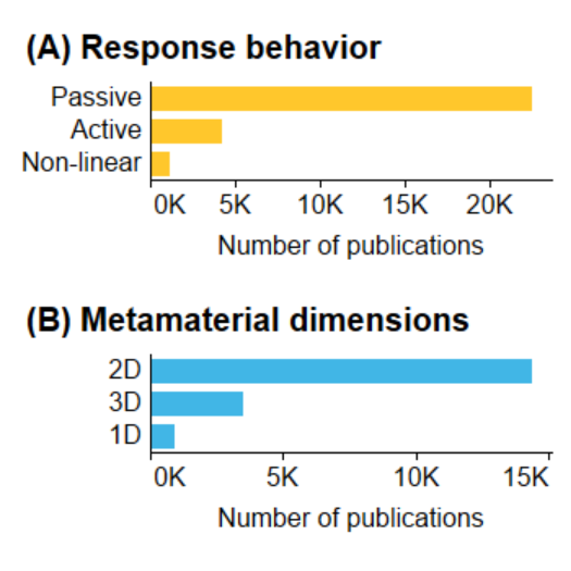
The response behavior classification reveals (Figure 5A) the field's current limitations and future trajectory. Passive metamaterials dominate the dataset at about 80% of publications since they are simpler, more reliable, and require no external power or control circuitry. These advantages are essential for applications like structural color, radar absorbers, and thermal management.
Active metamaterials, despite their smaller share, represent a technologically important category enabling dynamic reconfiguration. The ability to dynamically reconfigure metamaterial properties enables applications like adaptive electromagnetic signatures, reconfigurable antennas, and smart windows that adjust thermal and optical properties based on weather and occupancy.
Because of their complexity, nonlinear metamaterials occupy a specialized niche in high-performance photonics, enabling harmonic generation, parametric amplification, and all-optical switching. However, nonlinear effects become increasingly important as metamaterials integrate with quantum technologies and ultrafast optical systems.
The dimensional breakdown shows (Figure 5B) that this field is dominated by 2D metasurfaces, which represent about 85% of all publications. 2D structures are generally more compatible with planar lithography and thin-film manufacturing than fully 3D bulk metamaterials, although large-area nanoscale metasurfaces can still present significant fabrication challenges. More fundamentally, many metamaterial functionalities, such as beam steering, phase control, and holography, require only surface interactions rather than volumetric effects, making metasurfaces sufficient for these applications.
3D metamaterials maintain a significant presence despite fabrication challenges, driven by applications requiring bulk properties or volumetric wave manipulation. Acoustic and mechanical metamaterials favor 3D architectures, where structural hierarchy and internal geometry determine macroscopic behavior. The modest but persistent representation of 1D metamaterials (about 5% of total publications) reflects specialized applications in waveguiding, antenna design, and certain acoustic systems.
Read free, weekly briefings authored by CAS scientists and technology experts. Get emerging trends, useful connections, and future opportunities at the intersection of science, technology, and innovation delivered to your inbox.
Future outlook for metamaterials
More than two decades after negative-index materials first captured scientific imagination, metamaterials are becoming an engineering platform. The foundational science underlying many leading metamaterial and metasurface platforms is now well established, although significant scientific challenges remain for active, nonlinear, programmable, quantum-enabled, and multifunctional systems.
As fabrication technologies improve and active, programmable architectures mature, the ability to design material functionality through structure rather than composition may become transformative for wave-based technologies. Near-term commercial opportunities are concentrated in metasurface optics for compact cameras and augmented-reality systems, low-profile antennas for satellite and mobile communications, advanced radar and sensing systems for transportation and security, and tunable electromagnetic surfaces for next-generation wireless infrastructure.
The functionality analysis shared here provides a roadmap for investment prioritization. Wave absorption and sensing applications appear among more commercially mature categories with relatively clear integration pathways. Active modulation and advanced control functionalities offer higher long-term value but require greater investment and longer development timelines.
Our materials analysis also highlights a critical choice: work within established material platforms that enable near-term manufacturing or invest in emerging materials that may enable breakthrough performance but require longer development. As the uses of metamaterials grow in telecommunications, consumer electronics, security applications, and beyond, we expect to see scalable, cost-efficient production increase as well.
Key takeaway