


Executive Summary
- Innovation has concentrated in East Asia. China leads both research output and patent filings, with South Korea and Japan close behind on patents. Western activity is substantially lower and increasingly academic rather than commercial.
- Performance gains now come from device engineering more than from new emitter chemistry. Tandem stacks, silicon backplanes, and structural design are doing more for efficiency and lifetime than novel molecules.
- A short list of ring systems does most of the work. Carbazoles, dibenzofurans, dibenzothiophenes, fluorenes, and anthracenes recur throughout the patent record, and nine of the ten most common metal-free systems can each fill several roles at once.
- Blue remains the limiting factor. Blue emitters degrade faster and run less efficiently than red and green, which forces higher drive currents and constrains display lifetime, color stability, and power consumption.
- Panels are becoming bidirectional platforms. Photodetectors built into or beneath the stack support fingerprint reading and under-display cameras, moving OLEDs from standalone display components toward multifunctional systems.
Significant potential for next-generation display and integrated optoelectronic applications
Organic light-emitting diodes (OLEDs) have emerged as a leading optoelectronic platform, owing to their high efficiency, tunable emission, and mechanical flexibility. This review analyzes approximately 86 thousand OLED-related documents from the CAS Content Collection™ spanning 2016 to 2026, a period chosen to capture recent developments in this rapidly evolving field. This data-driven study provides a comprehensive assessment of advances across multiple dimensions of OLED technology.
The application landscape indicates widespread commercialization in consumer electronics and display technologies, with expanding roles in lighting, automotive systems, wearable devices, medical technologies, and immersive platforms such as AR/VR.
Despite ongoing challenges related to emitter stability, efficiency roll-off, and manufacturing complexity, emerging approaches in data-driven materials discovery and scalable fabrication are expected to enable further performance enhancements.
Organic light-emitting diodes (OLEDs) are electroluminescent devices that convert electrical energy into light, using organic molecules (or in some cases, metal complexes). Unlike conventional light emitting diodes (LEDs), which function as point light sources, OLEDs are area light sources that can be fabricated into various shapes and can even be made transparent and flexible, allowing them to be used in displays in devices such as televisions, computer and tablet screens, phones, heads-up displays, virtual reality systems, and lighting.
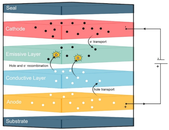
In OLEDs, electrical energy is converted into light through the injection of electrons and holes from opposite electrodes, maintaining charge neutrality. These charge carriers recombine in the emissive layer to form excitons that decay via fluorescence (singlet states) or phosphorescence (triplet states), with efficient devices using both pathways through intersystem crossing mechanisms. Structurally, OLEDs comprise multilayer thin films between an anode and cathode including charge generation layers, charge transport layers (hole-transporting and electron-transporting), and an emissive layer where controlled recombination and light emission occur. The general structure of an OLED is shown in Figure 1.
The evolution of OLED emitters has progressed through four generations marked by improved exciton utilization. Early fluorescent emitters were limited by spin statistics, harvesting only singlet excitons, whereas phosphorescent systems enabled near-unity internal efficiency by using singlet and triplet excitons via ISC. More recent generations employ thermally activated delayed fluorescence (TADF) materials, which exploit small singlet-triplet energy gaps (ΔEST) to enable RISC and convert non-emissive triplet states into emissive singlets. Building on this concept, fourth generation emitters, often known as hyperfluorescent emitters, combine TADF sensitizers with conventional emitters to achieve efficient exciton harvesting and high color purity. Control of ΔEST, primarily through the modulation of HOMO-LUMO overlap via donor-acceptor design and molecular geometry, is central to optimizing TADF performance.
At the device level, OLED performance is governed by multilayer architectures that control charge injection, transport, recombination, and light extraction. Modern OLEDs incorporate tandem architectures (stacked emissive units); micro-OLEDs (high pixel density on silicon backplanes); and transparent or flexible configurations, all of which have played a central role in improving efficiency, lifetime, and luminance. Additionally, innovations in pixel-level control, backplane technologies, and color-generation strategies have enabled specialized device configurations optimized for distinct applications. Increasingly, performance gains arise from system-level integration of electrical, optical, and mechanical design alongside materials innovation.
These technological developments are closely tied to the growing application landscape of OLEDs. OLED displays are now used in premium consumer electronics due to their high color fidelity and contrast, while their inherent flexibility and low power consumption make them suitable for wearable and medical devices. In automotive and AR/VR systems, OLEDs offer fast response times, high dynamic range, and adaptability to constrained or curved surfaces. Beyond displays, OLED-based lighting and emerging integrated systems, combining sensing, touch, and photonic functionalities, highlight the transition of OLEDs from standalone components to multifunctional platforms.
In this review, we analyze approximately 153 thousand OLED-related documents from the CAS Content Collection, the largest human-curated repository that encompasses publications from thousands of journals worldwide across diverse disciplines, as well as patents from 19 patent authorities, for the years 2001 to 2026. We provide comprehensive analysis from multiple perspectives: global research trends and intellectual property landscapes; materials innovation through detailed structural motif analysis, examining how specific molecular building blocks, such as carbazoles, dibenzofurans, fluorenes, and boron-containing heterocycles, which govern charge transport, exciton management, and emission across device layers; device architectures and engineering strategies; the relationship between material design and device implementation, highlighting how prevalent motifs are deployed across dominant OLED platforms; application landscapes; and key challenges with future directions including AI-driven materials discovery and scalable manufacturing.
Through this integrated perspective, the review aims to provide a fundamental understanding and a data-driven overview of the factors shaping the current state and future trajectory of OLED technology.
Ask complex, multi-part questions and receive context-based, cited answers sourced from 150+ years of curated and human-verified science found in the CAS Content Collection, making CAS Newton℠ the best agentic AI for science.
By the numbers
In this review, we analyze approximately 153 thousand OLED-related documents from the CAS Content Collection as well as patents from 19 patent authorities, for the years 2001 to 2026.
Trends in OLED research
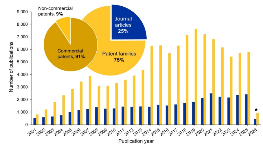
The publication trends for 153 thousand documents related to OLEDs were extracted from the CAS Content Collection for the period of 2001 to 2026 (Figure 2). We observed that the publication activity of OLEDs has evolved over time, growing substantially from the early 2000s through the late 2010s, reaching peak levels around 2019 to 2021, before declining moderately in subsequent years. Patent activity has declined sharply post-2020 while journal publications remain relatively stable, suggesting OLED technology has entered a mature phase focused on optimization rather than breakthrough innovation.
Notably, the distribution of publication types reveals that patents dominate the landscape, constituting 75% of all OLED-related publications, with commercial patents representing 91% of patent activity. This heavy emphasis on patent filings underscores the highly commercial and competitive nature of OLED technology development, where securing intellectual property rights has been prioritized over open academic publication. The relatively modest proportion of journal articles (25%) suggests that much of the innovation has been proprietary and industry-driven rather than emerging from fundamental academic research.
Global landscape of OLED innovation
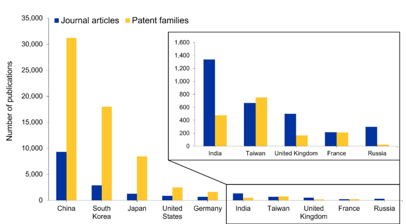
Analysis of the global OLED research and innovation from 2016 to 2026 (86 thousand documents) reveals strong geographic concentration in East Asia (Figure 3). China leads in both journal articles and patent families, reflecting coordinated national strategy integrating fundamental research with aggressive IP development. South Korea and Japan maintain high patent activity consistent with their mature OLED manufacturing ecosystems. In contrast, Western countries such as the U.S. and Germany show substantially lower activity, suggesting a relative retreat from mainstream OLED development or a strategic shift toward niche applications. Among smaller contributors, India emphasizes academic publishing with limited patenting, Taiwan demonstrates balanced research and IP output, while the U.K., France, and Russia exhibit academic presence but minimal commercial engagement. These patterns indicate that global OLED innovation is shaped by regional manufacturing capacity, reinforcing a divide between market-driven leadership and primarily academic participation.
Academic leadership in OLED research and IP
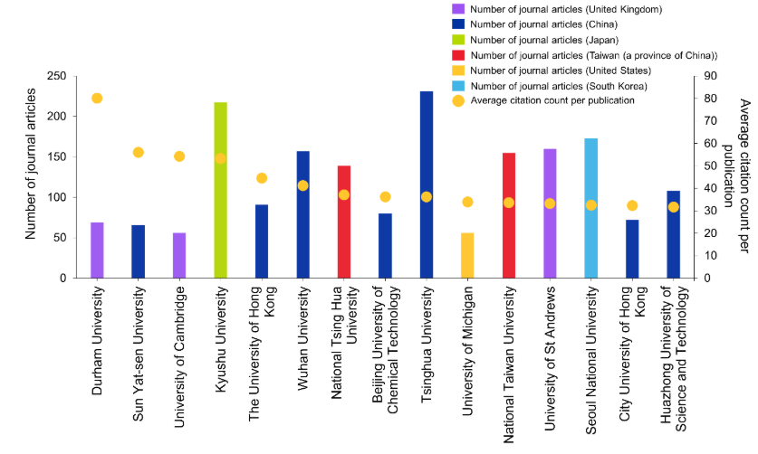
Leading academic institutions assessed by publication volume and average citation impact (Figure 4) reveal divergent research strategies. East Asian institutions, particularly China, Japan, South Korea, and Taiwan, dominate publication output, with Tsinghua University, followed by Kyushu University and Seoul National University leading in volume. However, Western institutions such as Durham University and the University of Cambridge show disproportionately high citations despite lower output, suggesting that OLEDs are a secondary research topic in academic institutions, but one that has provided disproportionate advancements.
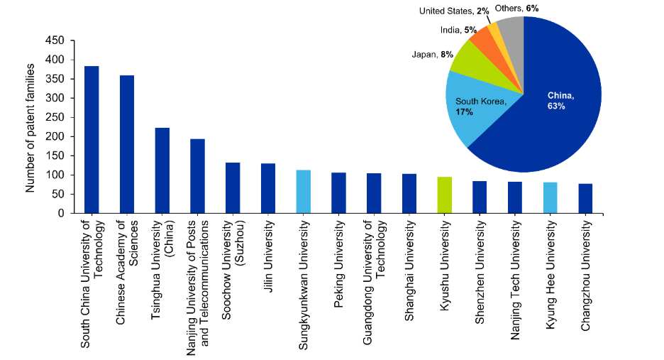
Non-commercial patent analysis (2016 to 2026; Figure 5) reinforces this geographic concentration. South China University of Technology and the Chinese Academy of Sciences lead in patent volume, with multiple Chinese universities (Tsinghua, Soochow, Jilin, and Nanjing University of Posts and Telecommunications) appearing prominently, indicating a systematic academic innovation ecosystem. South Korean and Japanese universities rank next, while U.S. and Indian institutions are notably absent from the top 15, signaling a significant shift in the global academic centers driving OLED innovation.
Leading and emerging corporate enterprises in OLED intellectual property
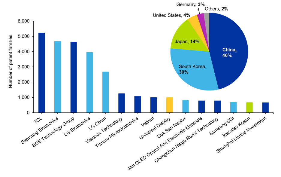
Commercial patent activity is concentrated among major East Asian corporations (Figure 6). TCL, Samsung Electronics, and BOE Technology Group emerge as clear leaders followed by LG Electronics and LG Chem. East Asian dominance is pronounced: China accounts for nearly half of all patent families among top assignees, South Korea represents the second-largest share, and Japan maintains significant presence. Western representation is minimal: Universal Display stands as the sole U.S. company among top patent assignees. This geographic concentration reflects a fundamental shift in innovation centers, with established infrastructure, supply chains, and technical expertise now concentrated in East Asia.
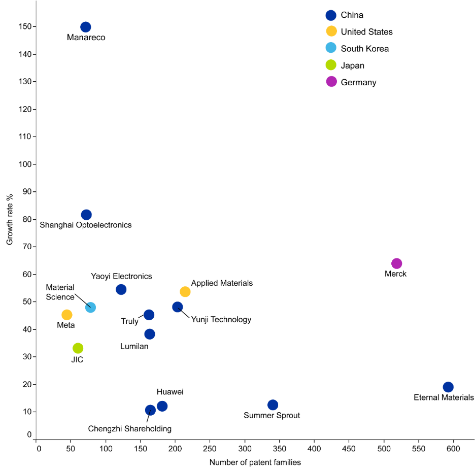
To find the emerging players in the field of OLED innovation, we evaluated the growth rate of commercial patent assignees between 2021 to 2025 (Figure 7). Our analysis revealed a pronounced dominance of Chinese enterprises among emerging players in this sector. Notable Chinese entities include Manareco, which exhibits extraordinarily high growth rates despite moderate patent holdings, and Shanghai Optoelectronics, also demonstrating strong growth momentum with similar patenting activity. Other Chinese players such as Yaoyi Electronics, Truly, Lumilan, and Yunji Technology operate at moderate growth levels with varying patent portfolio sizes, while Summer Sprout, and Eternal Materials represent less growth rate with extensive patent families. This concentration underscores China's strategic focus on establishing leadership in display technology and next-generation electronics manufacturing. In contrast, representation from other major technology-producing nations remains limited, with the United States represented by Meta, and Applied Materials; South Korea by Material Science; Japan by JIC; and Germany by Merck. This disparity suggests that emerging innovation activity in OLED technology is concentrated in China, while Western and other Asian markets may be experiencing barriers to new player entry or a consolidation of research activities within pre-existing corporate structures.
One missed patent reference can invalidate years of R&D investment. CAS IP Finder, powered by STN®, gives you comprehensive coverage and precision search tools in one intuitive platform—so you never miss what matters.
Key takeaway
Overall, the distribution highlights that OLED research and innovation gravitate toward applications in which its intrinsic properties can be efficiently leveraged, emphasizing domain-specific adoption pathways over uniform applicability across all display technologies.
Materials innovations driving OLED performance
OLED compounds are designed with distinct structural components that work synergistically to achieve efficient light emission. A clear understanding of how these molecules are divided into functional motifs is essential for rational material design and device performance optimization. In this study, we extracted all indexed substances from patents published over the most recent three-year period (2023 to 2025), enabling a focused analysis of trends across most common functional motifs used in a commercial OLED landscape seen in Figure 8. This data was used to identify seven main functions taken by the various motifs present in OLED compounds (Table 1): core chromophore/central units, donor groups, acceptor groups, linker/bridge units, peripheral/substituent groups, steric control groups, and ancillary ligands in metal complexes. Figure 8 focuses on motifs with ring systems larger than 3. For brevity, some smaller motifs with shown significance will only be briefly mentioned in Table 1.
Table 1: Seven main functions taken by motifs present in OLEDs
Patent landscape analysis: Structural motif prevalence and functionality
In this section, we analyze the structural motifs identified in Figure 8, which were created by dividing all indexed substances from patents published from 2023 to 2025 into two main categories: metal-free and metal-containing. This distinction separates conventional organic OLEDs from phosphorescent OLED materials based on transition metal organometallic complexes, which can be more expensive and have their specific needs and challenges. Within each category, motifs are further grouped by elemental composition: structures containing only C, N, O, or S atoms (Panel A and D), metalloid-containing species (Panel B and E), and compounds with other heteroatoms (Panel C and F).
Metal-free motifs
The patent analysis of metal-free OLED compounds containing only carbon, nitrogen, oxygen, and sulfur atoms (Figure 8, Panel A) reveals a clear hierarchy of structural motifs reflecting their versatile functionality in molecular design. Dibenzo[b,d]furan (A1) emerges as the most prevalent motif found in 176 thousand substances (in 3.1 thousand patents). It functions as a core chromophore and donor group because of the electron-rich furan ring that elevates HOMO levels and facilitates hole transport. Its rigid, oxygen-bridged structure provides critical steric control through three-dimensional non-planar geometry that resists intermolecular aggregation, which is essential for maintaining high quantum yields in solid-state films.
9H-Carbazoles (A2), present in 142 thousand substances and patents higher than dibenzo[b,d]furan (A1) at 3.5 thousand are widely used donor groups in hole-transport layers and host materials because of their electron-rich nature from nitrogen lone-pair delocalization. They enable strong electron-density and versatile functionalization through Buchwald-Hartwig coupling and SNAr reactions, and act as core chromophores, supporting complex donor-acceptor architectures through additional substitution at nitrogen.
9H-fluorene (A3) and 9,9'-spirobifluorene (A7) provide rigidity and steric bulk critical for emissive performance. Fluorene serves as a common blue-emitting scaffold and high-triplet-energy host, while spirobifluorene maintains fluorene’s electronic properties but enforces orthogonal ring orientation, yielding a 3D structure that limits packing and preserves high triplet energies for blue phosphorescent hosts.
Dibenzo[b,d]thiophenes (A4) offer tunable photophysical characteristics similar to dibenzofurans, with sulfur enhancing spin-orbit coupling to reduce ΔEST, improving quantum efficiency while enabling HOMO/LUMO optimization and preserving the beneficial steric and morphological properties.
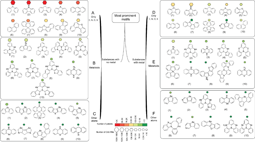
This metal-free category (only C, N, O, or S) also contains tricyclic aromatics anthracene (A5) and phenanthrene (A6), as well as triphenylenes (A9), which function as core chromophores with multiple points of attachment and allow linker and bridge functionalities with extended conjugation. Substituted anthracenes such as 9,10-diphenylanthracene (CAS RN® 1499-10-1) are also emissive and are commonly used. Naphthobenzofuran isomers (A8 and A10) extend conjugation while maintaining the electron-donating oxygen atom and rigid non-planar geometry of dibenzofurans and preserve its electron-donating and steric properties.
Nine of the ten most common ring systems found can act as core chromophores or linkers, secondary donors, or steric controllers, allowing a limited number of compact, synthetically accessible frameworks to perform multiple functions.
Metalloid-containing motifs
Boron and silicon incorporation represents a transformative strategy for creating electron-deficient molecular architectures addressing efficient electron transport and acceptor functionality, as shown in Figure 8 (Panel B). Boron-containing motifs dominate with nine of ten structures featuring boron centers, leveraging empty p-orbitals to accept electron density and promote charge delocalization. Polycyclic boron-nitrogen frameworks underpin multiple resonance TADF (MR-TADF) emitters, where special HOMO/LUMO separation minimizes ΔEST while maintaining narrow emission bandwidths for high color purity, particularly in blue OLEDs. A key example, 5,9-dihydro-5,9-diaza-13b-boranaphtho[3,2,1-de]anthracene (B1), illustrates this design: It combines an electron-deficient boron acceptor with a rigid anthracene core chromophore and ladder-type B-N coordination yielding a 3D structure that suppresses aggregation and narrows emission. Substituting N with O or S further tunes properties: B-O enhances stability, while B-S bonds offer unique orbital interactions which influence the (reverse) intersystem crossing rates critical for triplet harvesting. The bis-carbazole-boron complex ring system (B4) is an example of the donor-acceptor-donor architecture, where electron-deficient boron functions as an electron acceptor and a linker connecting carbazole donors, creating separated intramolecular charge-transfer states which are necessary for TADF. The boron-bis(carbazole) core embodies the fundamental design principles of TADF emitters.
Silicon motifs, exemplified by 5H-dibenzo[b,d]silole (B2), and azasiline (B9), provide complementary functionality through different electronic and structural effects. Siloles act as linker units in which silicon interrupts π-conjugation between aryl groups while providing steric control. They also exhibit σ*-π* interactions, where silicon σ* orbitals couple with π* systems to lower LUMO energy without significantly affecting HOMO levels, enabling efficient electron transport while preserving large band gaps for blue emission. Silanes can also improve the stability of emitters; silyl groups can block reactivity at positions otherwise susceptible to oxidation reactions that degrade an emitter.
The longer C-Si bond length (relative to C-C) changes bond angles, molecular geometry, and the conjugation between separated arenes; Silicon substituents can also prevent aggregation and undesired phase separation, improving processability and making manufacturing OLED potentially easier. Siloxane rings as substituents allow a larger number of substituents and greater separation between emitters, reducing their interactions with one another (such as triplet-triplet annihilation) and thus improving their emission efficiency. Azasilines combine silicon's bridging functionality with nitrogen's donor character, creating balanced electronic structures suitable for hole and electron transport. Silicon's tetrahedral geometry prevents planarization facilitating excimer formation while increasing the horizontal molecular orientation of films which maximizes light outcoupling by preferential transition dipole alignment.
Metalloid motifs provide strong acceptor character and three-dimensional control complementing donor-rich planar C/N/O/S motifs, together offering balanced charge transport, tunable energy levels, and controlled packing essential for high-performance devices across the visible spectrum.
Other heteroatom motifs
The presence of heavier main-group heteroatoms such as selenium and phosphorus alters the electronic and photophysical properties of OLED materials, as illustrated in Figure 8 (Panel C). Although less represented than C/N/O/S- or metalloid-containing compounds, they provide targeted advantages. Seven of the ten most common motifs containing heavy or unusual atoms contain selenium, indicating its usefulness in facilitating RISC through heavy atom-enhanced spin-orbit coupling and its value for phosphorescent emitters and TADF materials.
Dibenzo[b,d]selenophene (C1), the top motif of this group, functions as a core chromophore analogous to dibenzothiophene and dibenzofuran, while providing enhanced donor character and increased spatial steric bulk from selenium’s larger atomic radius. Extended frameworks combining selenium with oxygen (C2) or sulfur (C4) offer tunable HOMO levels and properties intermediate between all-selenium and all-sulfur/all-oxygen rings. In these systems, the differing atomic sizes of selenium and sulfur create controlled structural distortions that influence electronic structure and packing. The selenaborinine (C6) ring system combines boron's acceptor functionality with selenium's heavy atom properties, merging electron-deficient character for electron transport with enhanced spin-orbit coupling for triplet harvesting.
Phosphorus motifs, though less prevalent, are electronically versatile due to multiple oxidation states and coordination geometries. In its reduced (P(III)) form, 5,10-dihydroacridophosphine (C10) functions as an electron-donating linker or bridge, with tetrahedral geometry that suppresses planar stacking. In its oxidized form (P(V)) as phosphine oxide (P=O), the system becomes electron-accepting, lowering LUMO levels to facilitate electron injection and improving thermal stability, and is used in electron-transport materials. For example, spiroacridophosphines (C3) combine orthogonal spiro geometry with a phosphorus heteroatom, preventing aggregation while maintaining high triplet energies for blue phosphorescent hosts, and is used in electron-transport materials.
The limited patent representation of phosphorus and selenium compounds in OLED reflects their limited use, which likely stems from difficulties in the synthesis and handling of selenium compounds and the toxicity of selenium; they are likely most useful for specific challenges rather than as general-purpose building blocks.
Metal-containing complexes
Metal-containing compounds based on iridium(III) and platinum(II) phosphorescent complexes reveal how C/N/O/S structural motifs adopt different functional roles in coordination compounds (Figure 8, Panel D). This panel consists of ligand components rather than metal complexes with all ten prevalent motifs primarily serving as ancillary ligands, fine-tuning emission color, quantum efficiency, and electrochemical properties. Dibenzo[b,d]furan (D1), and 9H-carbazole (D2), maintain dominant positions but now modify photophysical properties of metal centers, with dibenzofuran providing extended π-conjugation for emission tuning while carbazole raises HOMO levels improving hole injection. Carbazole units are frequently substituents for phenylpyridine frameworks, tuning frontier orbitals without disrupting metal coordination. 9H-Fluorene (D3) serves as a blue-emission core chromophore while allowing attachment of ancillary ligands such as acetylacetonate, with the resulting orientation preventing triplet-triplet annihilation at high dopant concentrations.
Functional diversification arises from the contrast between donor and acceptor structures within ligands of metal-containing C/N/O/S complexes as shown in Figure 8 (Panel D). Dibenzo[b,d]thiophene (D4) offers unique tuning through sulfur-metal d-orbitals interactions that influence charge transfer and ligand-centered excited states governing emission and decay rates. In contrast, nitrogen-containing fused systems such as benzofuro[2,3-b]pyridine (D5) and benzo[4,5]thieno[2,3-c]pyridine (D9) act as electron-deficient acceptors. Benzofuro[2,3-b]pyridine (D5) enables blue-shifted emission through its pyridine nitrogen and oxygen-containing framework, maintaining high triplet energies. On the other hand, benzo[4,5]thieno[2,3-c]pyridine (D9) functions as strong-field cyclometalating acceptor with high quantum yields, where pyridine coordination and sulfur-driven π-extension tune emission toward longer red-shifting emission wavelengths.
Spirobifluorenes (D8) provide steric control for phosphorescent emitters with long excited-state lifetimes vulnerable to bimolecular annihilation, suppressing triplet-triplet annihilation and triplet-polaron quenching and improving efficiency and stability. Extended aromatics such as anthracene (D6) and phenanthrene (D10) serve similar purposes in metal-containing and metal-free emitters. Phenanthrene's bent geometry creates different packing and excited-state properties from linear anthracene, improving control over solid-state photophysics. Although less prevalent due to synthetic complexity, these ligands enable efficient harvesting of singlet and triplet excitons via metal spin-orbit coupling, improving internal quantum efficiency over fluorescent emitters.
Integration of metalloids into metal complex ligands is a strategy to combine the triplet harvesting of heavy metals with the properties of boron and silicon atoms, as illustrated in Figure 8 (Panel E). All ten prevalent motifs serve as ancillary ligands, as distinguished from their metal-free counterparts and demonstrating context-dependent functional roles. 5H-Dibenzo[b,d]siloles (E1), function as linker/bridge moieties with silicon interrupting aryl-aryl conjugation, while σ*-π* interactions lower LUMO levels to improve electron injection and transport. Incorporated into complexes such as Ir(ppy-silole)₂(acac), they tune emission and quantum efficiency without disrupting metal coordination. Substituents control steric bulk to prevent quenching of long-lifetime phosphorescent emitters vulnerable to triplet-triplet annihilation.
Boron-containing motifs exploit its electron-deficiency to tune metal complex photophysics. B-N heterocycles, like E2, function as acceptor groups to lower HOMO/LUMO levels, valuable for blue-shifting emission with high triplet energies and saturated blue coordinates. Incorporation into ancillary ligands provides a mechanism to fine-tune ligands without redesigning them. Boronate esters, such as E5, offer enhanced stability versus B-N bonds while maintaining acceptor character, with B-O bonds providing robust linkages withstanding thermal and electrical stress. B-N-S heterocycles, E4, use sulfur’s d-orbitals to create unique metal-ligand interactions influencing charge transfer and excited states and their decay rates and quantum yields.
Silicon's larger atomic radius and tetrahedral geometry prevent close intermolecular contacts, suppressing triplet-triplet annihilation and triplet-polaron quenching which limit efficiency and stability. Spirocyclic silanes (E6) control the aggregation of emitters through steric effects, interrupting aryl-aryl conjugation while enabling σ*-π* conjugation, providing a method to improve phosphorescence. Azasilines (E3) and oxasilines (E10) combine silicon's interruption of conjugation with nitrogen or oxygen donors, creating segments with isolated but connected electronic segments, which are valuable for bipolar transport and facilitate electron and hole injection. Their lower occurrence in the dataset likely reflects the difficulty of synthesis and their utility in limited circumstances. Metalloid incorporation is a method to optimize ligand properties without complete redesign.
Selenium and phosphorus-containing ligands occurred infrequently in emitters (Figure 8, Panel F), primarily in cases where synergistic heavy atom effects between ligands and metals are necessary such as for challenging deep blue emitters requiring high triplet energies or red/near-infrared emitters where intersystem crossing efficiency decreases with extended conjugation. In metal complexes with the dibenzo[b,d]selenophene moieties (F1), which appear in 23 patents, these ligands act as chromophores with selenium's enhanced spin-orbit coupling versus lighter chalcogens but can also function as ancillary ligands. Selenophenopyridines, benzo[4,5]selenopheno[2,3-c]pyridine (F2), and their isomers (F7) function as core cyclometalating ligands for metal complexes such as Ir(Se-ppy)₃ or Ir(Se-ppy)₂(acac) to maximize selenium's effects on excited-state dynamics while providing additional acceptor properties, altering ring fusion yields distinct electronic structures despite identical compositions. Boron-selenium heterocycles including B-N-Se (F3), selenaborinine, Si-B-Se (F9), and B-di-Se (F10) merge boron's electronic character, selenium's heavy atom effects on spin-orbit coupling and thus ΔEST, and multiple resonance substructures to optimize emission.
Multi-heteroatom systems are uncommon in our analysis reflecting practical barriers including the toxicity and air-sensitivity of selenium and the difficulty of syntheses involving it, high cost, and the lack of need for its performance advantages in most applications. However, their presence in patents indicates their novelty and their utility for applications where additional performance justifies their complexity, such as in displays requiring extreme color purity or ultra-high efficiency, or for optical communications or bioimaging requiring extended near-infrared spectral coverage. Large selenium polycycles (F5) are useful for red and near-infrared emission because of their extended conjugation of red-shifts emission and reduced barriers to triplet formation for useful quantum yields at longer wavelengths. The limited number of phosphorus-containing motifs such as imidazole-phosphorus compounds (F6), contrasts with the prevalence of phosphorus in coordination chemistry, but reflects dataset focus on aromatic conjugated frameworks and not saturated phosphines. Imidazole-phosphorus ligands may either act as multidentate ligands with phosphorus (III) or as phosphine oxide, or phosphorus (V) may enhance the electron-accepting character without altering coordination. Collectively, this category of OLED materials is primarily used in specialized applications and not in broad applications.
Emerging structural trends
From the most prevalent fragments, several trends emerge. Common motifs such as carbazoles, dibenzofurans and dibenzothiophenes, anthracenes, and fluorenes are most widely used due to their synthetic accessibility, ease of functionalization, and applicability across multiple types and generations of OLED materials. Carbazoles are commercially popular for their use as inexpensive and accessible electron-donating components in OLED emitters. Anthracenes and spirobifluorenes are commonly applied in OLED patents as they can be used as peripheral and steric substituents, as well as cores. Dibenzofurans and dibenzothiophenes act as synthetically accessible electron-donating substituents with stability, while phenanthrenes and fluorenes provide increased delocalization, leading to their popularity in the publication landscape. The prevalence of boron-containing materials in multiply fused ring compounds indicates the adoption of MR-TADF materials in commercial OLEDs. We cannot distinguish from their presence whether the materials are used as emitters themselves or as dopants for energy transfer to emitters. Selenium is by far the most common heavy element in OLED materials analyzed and is also consistent with incorporation in TADF materials where its mass and enhanced spin-orbit-coupling can influence excited-state dynamics and may improve efficiency and performance. Metal-containing OLED materials use similar ring systems to materials lacking metals. Nitrogen is incorporated in dibenzofuran and dibenzothiophene rings to allow direct coordination to metals, while silicon-containing ring systems are more common as well. Overall, these observations highlight how prevalent molecular design strategies shape the material landscape, motivating an examination on how device architectures leverage these structural features in practical OLED systems.
Device architecture and performance enhancements
As OLED technologies mature beyond simple emissions, device differentiation arises from how optical, electrical, and mechanical design choices are integrated. To analyze this evolving landscape, we used CAS-indexed controlled terms to identify documents related to device architecture and technologies and examined approximately 25 thousand OLED device technology-related documents and classified technologies based on their function in an OLED stack, encompassing the substrate, pixel control layer, emission layer, color conversion/filter layer, integrated system layer, and encapsulation.
OLED architecture landscape
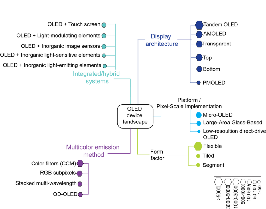
This classification reveals a multi-dimensional, orthogonal design space in which innovations occur across five primary dimensions: display architecture, platform and pixel-scale implementation, color generation strategy, physical form factor, and system-level integration as seen in Figure 9. Rather than fitting into a linear taxonomy, modern OLED devices emerge from specific combinations of choices across these layers, enabling diverse realizations optimized for applications ranging from large area displays to ultra-high-resolution micro-displays and low-power indicator panels.
Display architecture
Within this framework, display architecture captures the structural and electrical decisions that govern pixel addressing and light generation. Tandem OLEDs act as performance enhancers rather than standalone addressing architectures, applicable across active-matrix OLEDs (AMOLED), top-emission, and transparent configurations, as reflected by its occurrence across multiple device categories in the underlying data. They employ multiple electroluminescent units (typically two-to-three layers) that are vertically stacked and electrically connected in series within a single pixel, enhancing luminous efficiency and extending operational lifetime at equivalent brightness levels. Unlike conventional single-unit OLEDs, tandem architectures incorporate two or more emissive stacks separated by charge-generation layers (CGLs) that enable efficient carrier recombination at each internal interface. Ytterbium (Yb)-based CGLs features as one of the prominent inventions in the technology landscape of tandem OLEDs. Yb is especially effective in tandem OLEDs because it forms stable charge-transfer complexes that create internal, low-loss electron reservoirs within the n-type CGL, enabling efficient and durable charge generation for stacked electroluminescent units. From an architectural perspective, tandem OLEDs exemplify a shift from materials-centric performance scaling toward device-level engineering, where electrical stress is redistributed across stacked emissive units rather than mitigated solely through new emitters.
AMOLED and passive matrix OLEDs (PMOLED) constitute the two electrically distinct base architectures within this category. AMOLEDs use thin-film transistor (TFT) backplanes that enable independent pixel control, high refresh rates, and scalability to high resolutions and large areas. In contrast, PMOLEDs rely on passive row-column addressing without pixel-level switching, constraining their use to small-format, low-resolution applications. Correspondingly, AMOLED nodes dominate this branch by document volume in Figure 9, while PMOLED appears as a comparatively minor category.
AMOLED research has mainly concentrated on the transition from inorganic to organic backplane insulators and structures. Additionally, research also focuses on emission technology through manufacturing methods such as inkjet-printed RGB OLEDs. The patent landscape is dominated by inventions that optimize how light is generated, confined, extracted, and protected within the OLED stack, particularly for flexible and silicon-based micro-OLED applications. This highlights a shift toward photon and system-level engineering as OLED technologies mature. This branch also includes optical architectural variants, namely bottom-emission, top-emission, and transparent OLEDs (bidirectional or selective emission), each optimized for specific optical requirements.
This illustrates how OLED innovation has shifted from basic addressing schemes toward stack-level and photon-management strategies, setting the foundation for downstream differentiation across platform implementation, form factor, and system integration.
Platform and pixel-scale implementation
This dimension in Figure 9 describes how OLED pixels are fabricated, addressed, and scaled, directly constraining achievable resolution, brightness, power density, cost, and target applications. Micro-OLEDs fabricated on silicon complementary metal-oxide (CMOS) backplanes represent the most document-intensive platform, driven by their importance for high-resolution near-eye displays. In this architecture, OLED emissive stacks are deposited directly onto processed silicon wafers, enabling sub-micron pixel pitches but introducing stringent manufacturing and yield constraints.
Micro-OLED innovations have centered on incremental changes in manufacturing and materials rather than on the development of entirely new materials. Research focuses includes yield improvement and defect reduction through protective structures around metal interconnects (e.g., indium tin oxide (ITO) sidewall coatings), multilayer encapsulation schemes, and adhesion optimization for high-density patterning. A secondary but visible cluster of documents is centered on optical performance, particularly the reduction of inter-pixel optical crosstalk and color mixing at extreme pixel densities.
Smaller nodes in this branch, including large-area, glass-based, and low-resolution, direct-drive OLEDs capture exploration approaches that combine complementary technologies to overcome OLED's intrinsic limitations. Large-area glass-based OLEDs are active-matrix displays fabricated on glass substrates using TFT backplanes, enabling high-resolution, full-color panels for applications such as smartphones and televisions. Recent research focuses on simplified architectures and improved RGB efficiency for scalable manufacturing, including hybrid micro-LED/OLED architectures that employ inorganic LEDs to address blue emission constraints. In contrast, direct-drive OLEDs are segmented architectures in which discrete emission regions are independently powered without a matrix backplane, making them suitable for low-resolution displays and lighting applications. Innovation centers on optical and structural optimization of individually driven segments, particularly through refractive index engineering to reduce losses and improve luminance uniformity. Despite their lower representation, these approaches highlight how platform-level integration can balance performance trade-offs beyond emitter-level design.
Form factor
In OLEDs, form factors describe physical configurations such as flat, curved, foldable, thin, or flexible designs. The branch is dominated by flexible OLEDs (Figure 9), reflected by the largest node size in this segment. This prominence arises from sustainable effort to achieve mechanical compliance without sacrificing electrical or optical performance. A key focus is the replacement of brittle ITO with flexible electrodes that maintain high conductivity, transparency, and mechanical robustness under repeated bending.
Achieving flexibility extends beyond substrate substitutions with polymers and requires coordinated engineering across materials, mechanics, optics, and interfacial layers. Structural strategies such as Cu-Be serpentine interconnects increase strain tolerance by up to ~200% compared with conventional straight conductors. At the materials level, composite charge-transport layers, for example poly[N,N′-bis(4-butylphenyl)-N,N′-bis(phenyl)benzidine]:4,4′,4″-tris(carbazol-9-yl)triphenylamine (poly-TPD:TCTA) architectures used in red CsPbI₃ perovskite-based emissive systems have been shown to retain ~80% of their initial external quantum efficiency after 300 bending cycles. Architectural approaches, including stretchable designs with rigid OLED islands interconnected by flexible links, further decouple mechanical compliance from electronic function.
Additional form factors include tiled and segmented displays. Tiled OLED displays are formed by combining multiple smaller OLED panels into one large, scalable screen, enabling the creation of large displays while minimizing visible seams between modules. Segmented OLED displays, in contrast, divide a panel into predefined regions or segments that can be independently controlled. These are typically used to display simple icons, numbers, or symbols efficiently. Research on tiled OLED displays focuses on driving schemes to reduce distortion between tiled panels which address synchronization and scan delay issues in modular OLEDs. Segmented OLED advancements have been developed such as power-optimized OLED architectures for wearables and improving energy efficiency improvements through localized control strategies.
Overall, these approaches highlight a key trend: mechanical resilience is achieved through structural and geometric design rather than fully flexible materials. The dominance of flexible OLEDs underscores the importance of system-level mechanical integration in advancing form-factor innovation.
Multicolor emission method
The Multicolor emission branch in Figure 9 highlights the main strategies for achieving RGB output in OLED platforms, with node size reflecting technical maturity and manufacturability. The Color Filter Method (CCM), based on blue or white OLED emission combined with color filters or conversion layers, remains widely used despite its intrinsic optical losses (~60-70%). Recent advances including optical-cavity tuning, refractive-index-matched capping layers, and photoluminescent color filters can partially recover efficiency.
RGB subpixel patterning forms a second major approach, driven by advances in photolithography-compatible organic and quantum-dot (QD) patterning. Resolutions exceeding 1000 PPI and ligand-engineered QD photoresists retain ~70% photoluminescence following lithographic processing demonstrating progress toward ultra-high-density displays. Pure QD color-conversion architectures, relying on blue excitation without filters or lateral patterning, represent a smaller but performance-intensive category. Optical enhancements such as mixed-shape scattering layers and plasmonic structures have achieved up to sevenfold red output gains and ~90% conversion efficiency, albeit with ongoing stability challenges.
Tandem or stacked multi-wavelength OLEDs generate multicolor emission by vertical spectral-engineering strategy rather than by generating many distinct colors, enabling intrinsic white emission, tunable color balance, and wavelength narrowing without lateral patterning or external filters.
Overall, academic research addresses fundamental efficiency, exciton management, and optical modeling, whereas patent activity focuses on engineering solutions that enable high-yield manufacturing and stable color reproduction. Patent disclosures emphasize device-level suppression of residual blue leakage, via selective reflection or polarization-manipulation layers. They also highlight hybrid pixel concepts that replace unstable blue OLED emitters with QD-based blue emission while retaining organic red and green pixels.
Integrated/Hybrid technologies
The Integrated and hybrid technologies branch in Figure 9 captures a shift in OLED innovation: from optimizing isolated device components toward system level co design, where emission, optics, sensing, touch, and inorganic functionalities are engineered as a single, interdependent platform. Patent activity in this space indicates that OLED panels are no longer treated as self-contained light sources, but rather as structural hubs serving multiple functions without compromising brightness, color purity, or reliability.
Integration with touch functionality exemplifies this transition. Rather than adding discrete touch stacks, patents describe architectures that repurpose OLED electrodes as capacitive sensors, embed display-on-touch (DOT) layers, or combine touch, directional sound emission, and mechanical foldability within the same panel. These solutions primarily address manufacturing efficiency, reducing stack thickness, minimizing interfacial defects, and maintaining optical uniformity under mechanical deformation, highlighting how integration directly translates into yield and form-factor advantages.
A similar system level logic governs OLED incorporating light modulation. Patent disclosures emphasize replacing passive, standalone optical elements with engineered, multifunctional optical stacks, including microcavity control layers, cholesteric liquid-crystal cavities, wavelength-matched retardation films, and electrochromic metal-oxide layers. Unlike journal studies that often treat contrast, viewing angle, polarization, and color purity as separable optimization problems, these hybrid architectures tightly couple multiple optical functions, enabling displays that dynamically adapt emission spectrum, polarization state, and angular distribution in response to ambient conditions, often with reduced power consumption.
Sensor integration further reinforces the OLED panel’s evolution into a bidirectional optoelectronic platform. In under-display cameras and fingerprint sensing, early transparency-based approaches give way to more sophisticated architectures that locally modify pixel geometry, electrode transparency, light-transmission layers, microlenses, or stress-relieved through-structures. Increasingly, photodetectors are fabricated within or directly beneath the OLED stack, sharing electrodes or transport layers to simplify processing while preserving display performance. These designs blur the boundary between emitter and detector, positioning OLEDs as platforms that both generate and sense light.
Finally, hybridization with inorganic materials underscores how integration enables durability, scalability, and new application spaces. Inorganic barrier layers, silicon backplanes, metal-oxide functional films, transparent conductive oxides, metal nanostructures, and ultra-thin glass substrates emerge as core performance enablers rather than auxiliary layers. Silicon-based OLED micro-displays leverage CMOS precision for ultra-high pixel densities, while inorganic black matrices, electrochromic oxides, and reflective metal layers address crosstalk, ambient reflection, and brightness challenges that organic materials alone cannot resolve. This branch of the landscape demonstrates that as OLED technologies mature, differentiation arises from hybrid system architectures that ensure laboratory-level efficiency and lifetime gains remain viable in real-world products and high-volume manufacturing.
Overall, integrated and hybrid technologies illustrate a clear transition in the OLED field from isolated device innovation toward platform-level engineering. While journal articles define what is physically possible at the level of materials and device physics, patent activity shows how these possibilities are consolidated into manufacturable, multifunctional display systems, blurring the boundaries between display, sensing, optics, and materials engineering.
Frequent motifs used in predominant device technologies
Central to these system-level advances in Figure 10 is precise molecular electronic structure engineering, where recurring structural motifs are deployed individually or synergistically across various substances to govern charge transport, exciton formation, and light emission in support of specific platform functions. To examine the motifs most relevant to dominant device technologies, their frequencies were analyzed across two categories: (i) C/N/O/S-based functional motifs and (ii) motifs incorporating other heteroatoms.

Among conventional heterocyclic motifs, 1,3,5-triazine is the most prominent electron-deficient unit. Its nitrogen-rich aromatic core stabilizes charge transfer states, making it critical for tandem OLED CGLs and charge transport layers of AMOLEDs. Triazine derivatives facilitate efficient charge separation at p/n interfaces, enable exciplex formation with small ΔEST, and support p-type doping, collectively ensuring low-loss charge generation. Across patents, triazine and related acceptor motifs consistently appear as foundational components of charge-generation architectures. 1,3,5-Triazines also possess multiple points of attachment for substituents, allowing a single molecule to serve multiple functions.
Naphthalene functions primarily as a π-conjugation extender and structural linker, widely used across transport layers and host systems. It enhances electron mobility and film stability, particularly in phenanthroline-based electron transport/charge generation material, highlighting its role as a modular backbone rather than an active electronic center.
Rigid fused motifs, such as dibenzofuran and fluorene, provide structural stability and high-triplet energy. Dibenzofuran contributes to thermal and morphological robustness and wide bandgap characteristics. In tandem OLED technology, the dibenzofuran moiety is a chiral ligand backbone in an Mn(II) complex, while in CGL compositions, it acts as a structural component in electron-accepting and hole-transporting molecules, which contributes to efficient charge generation and stability in tandem OLED architectures. Fluorene serves multiple roles across the OLED stack: as a π-conjugated bridge in emitter design, a rigid structural unit providing high triplet energy and thermal stability, and a high refractive index component in encapsulation systems. It also acts as a scaffold for deuterated transport and host materials. These functions arise from its rigid planar structure, tunable 9,9-substitution for morphology control, and compatibility with both solution and vacuum processing, making it a versatile building block.
Pyridine plays a multifunctional role, acting as (i) metal-coordinating ligand component in phosphorescent emitters, (ii) an electron deficient linker in organic architectures, and (iii) a tuning element for optical and electronic properties. These roles stem from pyridine's electron-withdrawing heteroaromatic character combined with its coordination capability, making it versatile for organometallic emitter design and organic layer engineering in OLED architectures.
Other common motifs: carbazole, dibenzothiophene, phenanthroline, pyrimidine, and other specialized heterocycles, represent targeted building blocks addressing specific functional requirements in tandem OLEDs and AMOLEDs. Carbazole is a dominant donor for hole transport and host design and is extensively used in p-doped CGLs, TADF emitter donor components, and chiral hole transport materials for circularly polarized emission applications. Dibenzothiophene provides sulfur-mediated rigidity with tuned electronic properties, lower triplet energy and modified HOMO/LUMO levels suitable for red/green hosts, while its heavy-atom effect enhances intersystem crossing. Phenanthroline functions both as a metal-chelating ligand in phosphorescent emitters and as an electron-transporting scaffold in n-doped CGLs, with rigid planarity and strong electron-accepting character enabling efficient electron injection when alkali-metal doped. Pyrimidine offers enhanced electron affinity compared to pyridine, serving in electron transport materials and bipolar hosts. Less prevalent motifs such as benzofuran-pyridine fused systems, benzo[k]xanthene, naphtho-benzoxazole, and tetrahydroquinolines are used in similar-volume applications including high refractive index capping layers, morphologically stable hosts, and sterically hindered transport materials for preventing aggregation.
These motifs provide heteroatom diversity (N, O, S) and structural variations enabling precise optimization of charge balance, exciton confinement, and interface energetics across complex tandem OLED and AMOLED architectures. Their moderate occurrence frequencies reflect their role as specialized optimization tools rather than universal building blocks, deployed strategically where specific properties are required.
Motifs with other ring atoms (Figure 10, right panel) represent a class of rigid polycyclic architecture incorporating main group heteroatoms (B, N, P, S, Se, Si, Ge) designed to optimize OLED performance. As discussed in the previous section, the most common framework features B as an electron acceptor paired with nitrogen donors, creating an intramolecular donor-acceptor architecture that spatially separates HOMO and LUMO orbitals. Further, heavy atoms such as Se and S enhance spin-orbit coupling for phosphorescent applications while systematic substitution of heteroatoms (P, Si, Ge) allows precise tuning of emission wavelengths across the visible spectrum. Together, these structural features create a versatile molecular platform that addresses the fundamental challenge of OLED technology: harvesting all electrically generated excitons while maintaining excellent color quality, stability, and device longevity.
These rigid heteroatom-rich polycyclic motifs are prevalent in tandem OLEDs and AMOLEDs because they enable near-unity exciton harvesting at low current densities while delivering narrow, cavity-compatible emissions. Their structural rigidity and tunable heteroatom chemistry also provide superior operational stability and energy-level control, critical for stacked architectures and pixel-driven displays.
The diversity of motifs reflects the complexity of OLED device physics, in which no single molecular structure can simultaneously optimize electron transport, hole transport, exciton formation, light emission, and charge generation. Instead, OLED technology requires a library of complementary molecular building blocks, each excelling in its designated role, working together in a carefully engineered multilayer architecture to achieve high performance.
Applications landscape of OLED technology
Key application areas of OLED devices
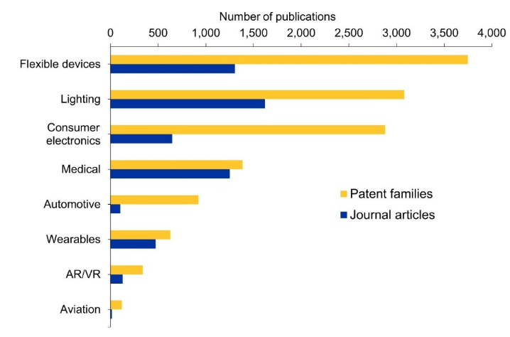
We analyzed application domains in OLED research to identify how research and patent activity align with end-use sectors, revealing where technological strengths, market pull, and commercialization readiness converge (Figure 11). Flexible devices dominate both academic and patent landscapes, reflecting OLED’s intrinsic advantages such as mechanical flexibility, lightweight structure, thin form factor, and low-temperature processing compatibility with plastic substrates. These attributes make OLEDs suited for foldable displays, rollable screens, and flexible electronics, explaining strong engagement from both researchers and industry. Lighting and consumer electronics also exhibit strong patent orientation, highlighting OLED’s commercial maturity in high-value displays like television, smartphones, laptops, tablets etc. and solid-state lighting, where high contrast ratios, wide color gamut, energy efficiency, and design freedom offer clear advantages over conventional technologies. In these domains, the concurrent presence of sustained journal activity and extensive patenting indicates that OLED technologies have advanced to stages where research and innovation are directed toward refinement, implementation, and application specific development rather than initial feasibility demonstration.
Medical and wearable applications show balanced but differentiated engagement, indicating growing interest in specialized use cases. OLEDs are well-suited for medical and wearable devices due to their low power consumption, eye-safe emission characteristics, and ability to be integrated into soft, body conformable platforms, enabling applications such as diagnostic and surgical displays, phototherapy panels, flexible health monitoring patches, smartwatches, and fitness trackers that require thin, lightweight, and compact display and light emission solutions. Automotive and AR/VR applications, while more selectively explored, leverage OLED’s fast response times, high dynamic range, and form factor versatility for displays in constrained or immersive environments. In contrast, aviation exhibits limited research and patenting activity, suggesting OLED research and innovation remain less extensive relative to other domains, potentially reflecting the stricter performance, integration, and qualification requirements inherent to this sector.
Overall, the distribution highlights that OLED research and innovation gravitate toward applications in which its intrinsic properties can be efficiently leveraged, emphasizing domain-specific adoption pathways over uniform applicability across all display technologies.
Co-occurrence between applications and OLED devices
To quantify OLED technology-application relationships, we analyzed co-occurrence patterns between device architectures and application domains. The heatmap in Figure 12 visualizes co-occurrence counts between individual OLED technology concepts (rows) and application domains (columns), with color intensity representing the frequency of joint occurrence. The statistical significance of technology-application associations was first evaluated using chi-square analysis, followed by correspondence analysis (CA) to capture underlying relational structure in the data space. Hierarchical clustering was then applied to both rows and columns based on similarity in co-occurrence profiles, grouping technologies and applications with shared usage patterns. Color bars along the rows indicate technology cluster membership, distinguishing specialized (Cluster 1) and mainstream (Cluster 2) groups.
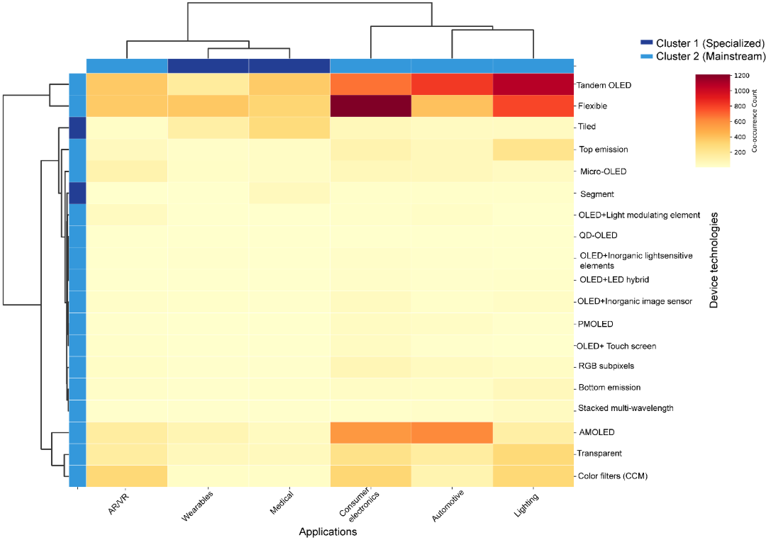
Hierarchical clustering revealed clear similarity patterns among the device technologies based on their co-occurrence profiles. The dendrogram indicates that technologies joining at lower linkage distances exhibit strong similarity, forming tightly connected groups, whereas those merging at higher levels reflect more distinct behavior. The specialized cluster is narrow, comprising only Tiled and Segment architectures, both of which show consistently low co-occurrence counts across all application domains, distinguishing them structurally from the rest of the technology set even though their absolute activity is modest. The remaining technologies, including micro-OLED, PMOLED, RGB subpixels, Tandem OLED, and Flexible, form the broader mainstream cluster. Within this mainstream group, Tandem OLED and Flexible stand out with markedly higher co-occurrence intensity, particularly with Consumer electronics and Lighting, indicating that linkage-distance similarity does not necessarily correspond to similar activity levels; two technologies can cluster together structurally while differing substantially in overall co-occurrence volume.
Tandem OLED and Flexible, despite belonging to the mainstream cluster, show the highest co-occurrence intensity in the entire heatmap, concentrated in Consumer electronics, Automotive, and Lighting, reflecting their broad adoption across high-volume application areas. Tiled and Segment, the two specialized-cluster technologies, show comparatively low and diffuse co-occurrence across all applications, without a sharply concentrated signal in any single domain. On the application side, Wearables and Medical form a distinct specialized cluster, while Consumer electronics, Automotive, and Lighting form the mainstream application cluster with generally higher co-occurrence counts across most device technologies.
The dendrogram structure therefore highlights a clear separation between a small set of low-activity, structurally distinct technologies (Tiled, Segment) and a broader mainstream group that includes both moderate-activity and high-activity technologies. This fine-grained structure provides mechanistic context for the enrichment patterns observed at the cluster level, illustrating how structural similarity in co-occurrence profiles does not always align with similarity in overall activity level, an important distinction when interpreting cluster-level enrichment and depletion signals.
Read free, weekly briefings authored by CAS scientists and technology experts. Get emerging trends, useful connections, and future opportunities at the intersection of science, technology, and innovation delivered to your inbox.
Challenges
Despite their remarkable advantages and widespread adoption in commercial displays, OLEDs continue to face several significant technical and economic challenges that limit their broader application and long-term viability. One of the most persistent issues is device lifetime and efficiency, driven by the inherent instability of organic electronic materials. Degradation from oxygen, moisture and operational stress leads to brightness loss and color shifts over time, with blue emitters degrading significantly faster than red and green. This imbalance affects color stability and limits overall device lifetime, especially under high brightness and temperatures (e.g., HDR or outdoor use). Blue OLEDs also exhibit lower efficiency, requiring higher drive currents that further accelerate degradation and increase power consumption. Additional losses from charge imbalance, exciton quenching, and light trapping further reduce real-world efficiency.
Manufacturing complexity and cost represent another major barrier. The production of OLED fabrication requires controlled environments with ultra-low humidity and oxygen levels, as even trace amounts of these contaminants can severely compromise device performance. Moreover, OLED fabrication requires precise multilayer deposition of extremely thin organic films, often under high vacuum conditions. Techniques such as vacuum thermal evaporation are expensive and result in significant material wastage, especially for large-area panels. Further, the reliance on rare materials like iridium and platinum in phosphorescent emitters further increases material costs and raises concerns about long-term supply chain sustainability. These manufacturing hurdles contribute to higher prices compared to mature display technologies like LCDs.
The phenomenon of burn-in or image retention poses yet another challenge for OLED displays, particularly in applications requiring static content. Differential pixel aging causes persistent ghost images. Despite various mitigation strategies, including pixel shifting, screen savers, and brightness management algorithms, burn-in remains a concern for professional monitors, signage applications, and consumer devices with persistent UI elements. This issue is problematic given the expectation of durable and uniform performance over the operational lifetime of displays.
Finally, material development and scalability issues continue to constrain technology’s potential. The discovery and optimization of new OLED materials with improved efficiency, stability, and color purity is a time-consuming and expensive process. TADF materials show promise as alternatives to phosphorescent emitters, potentially eliminating the need for heavy metals, but these materials often suffer from efficiency roll-off at high current densities and stability concerns. Additionally, scaling OLED technology to new form factors, such as transparent displays, flexible and foldable screens, or large-area lighting panels, introduces additional technical challenges related to substrate selection, encapsulation techniques, and maintaining uniform performance across large areas. The development of printable OLEDs that could dramatically reduce manufacturing costs remains confined to research laboratories, with significant obstacles preventing commercialization.
Together, these challenges highlight why, despite their superior contrast, color quality, and form-factor advantages, OLEDs remain an active area of research rather than a fully optimized, universal display solution.
Future outlook
The future of OLED technology will be defined by parallel advances across several interconnected fronts, including materials innovation, data-driven discovery approaches, emerging display architectures, specialized microdisplay platforms, and scalable manufacturing techniques. Among these, artificial intelligence (AI) is transforming the materials discovery process, accelerating traditionally slow, trial-and-error approaches. Publication trends show a steady rise in AI-driven OLED research, reflecting growing academic and industrial interest. Machine learning models, including deep neural networks, variational autoencoders (VAEs), and generative adversarial networks (GANs), enable rapid screening of molecular candidates and prediction of key photophysical properties such as emission wavelength, quantum yield, and stability prior to synthesis. This is impactful for addressing the long-standing challenge of stable, high-efficiency blue emitters with AI facilitating molecular design, ligand optimization, and degradation prediction, thereby shortening development cycles and accelerating commercialization.
Beyond materials discovery, OLED technologies are evolving toward more immersive display paradigms. Holographic OLEDs represent one such direction, combining self-emissive properties with advanced light-field or holographic optics. Rather than true volumetric holography, these systems generate depth-rich, three-dimensional visual effects through controlled light manipulation. Integration with holographic optical elements (HOEs), diffraction gratings, or light-field architectures enables floating or spatially realistic images without the need for glasses, making them attractive for AR, automotive head-up displays, medical visualization, and advanced human-machine interfaces.
Closely related to these immersive applications is the rapid advancement of OLED-on-silicon (OLEDoS) technology, which integrates organic emissive layers onto CMOS-based silicon backplanes. This architecture enables ultra-high pixel densities, fast switching, high current drive, and precise grayscale control, resulting in superior image quality and refresh rates. These features are critical for near-eye applications such as AR/VR, where even minor imperfections are magnified. With increasing demand for compact, lightweight wearable systems, OLEDoS is emerging as a key platform for next-generation human-computer interaction across consumer, medical, automotive, and defense applications.
At the manufacturing level, inkjet-printed OLEDs are gaining increasing attention as a cost-effective alternative to conventional vacuum thermal evaporation. Unlike vacuum processes requiring expensive equipment and shadow masks, inkjet printing enables mask-free, additive deposition with significantly improved material utilization. This makes it well-suited for large-area displays and lighting panels, where conventional methods become costly and inefficient. Its compatibility with flexible substrates and reduced capital investment further positions it as a critical enabler for scalable OLED production.
Overall, while OLEDs are unlikely to become a universal solution for all display and lighting applications in the near term, continued progress across materials development, AI-driven discovery, advanced display architectures, and manufacturing technologies are expected to mitigate many of their current limitations. The convergence of enhanced performance, novel form factors, and more economical fabrication methods suggests a future in which OLEDs play a more prominent and diversified role across consumer electronics, lighting, and emerging optoelectronic applications.
Conclusion
OLED technology has evolved from early conceptual demonstrations to a mature platform driven by advances in molecular design, device engineering, and system-level integration. This review analyzed ~86 thousand OLED-related documents from the CAS Content Collection (2016 to 2026), capturing recent developments in a rapidly advancing field. The innovation landscape shows strong industrial participation and geographic concentration of patents, particularly in East Asia, complemented by academic research focused on fundamental understanding and incremental improvements.
Materials innovation remains central, with recurring structural motifs, such as carbazoles, dibenzofurans, fluorenes, and boron-containing heterocycles, serving as modular, multifunctional building blocks across emitter systems and device architectures. These motifs enable precise control over charge transport, exciton dynamics, and emission characteristics, supporting continued gains in device performance and operational longevity.
Progress is shaped by advances beyond materials alone, including device architecture, hybrid integration, and scalable manufacturing. Developments such as tandem OLEDs, micro-OLED (OLEDoS) platforms, and flexible or transparent form factors reflect a shift toward application-driven optimization, enabling translation from laboratory concepts to real-world products.
As a result, OLEDs now span a broad application space, from consumer electronics to lighting, automotive interfaces, AR/VR, and emerging bio-integrated systems. Their compatibility with flexible substrates and integration with sensing and optical components further strengthens their role in next-generation multifunctional devices.
Despite this progress, challenges such as blue emitter durability and emission purity, and manufacturing complexity persist, necessitating continued interdisciplinary innovation. Emerging approaches, including AI-driven materials discovery, advanced device architectures, and cost-efficient fabrication, are expected to address these limitations.
Overall, OLED technology is transitioning from rapid innovation to strategic refinement, where coordinated advances across materials, devices, and systems will define future progress, sustaining its role as a versatile platform for next-generation optoelectronic applications.
---
Download a print-version of the report that also includes all references.
Conclusion