
.avif)

エグゼクティブサマリー
- ワイドバンドギャップおよびウルトラワイドバンドギャップ半導体は、バンド間のエネルギー分離が大きく高温・高出力の用途に適しているため、従来のシリコン半導体よりも優れた電気的・熱的性能を実現できます。
- 炭化ケイ素と窒化ガリウムは、これらの半導体材料として最も研究が進んでおり、特許文献では炭化ケイ素の方が一般的です。
- ワイドバンドギャップおよびウルトラワイドバンドギャップ半導体を使用した主要デバイスには、トランジスタ、発光素子、集積回路/メモリデバイスがあり、高強度環境に対応可能な半導体の必要性が示されています。
- 光エレクトロニクスとパワーエレクトロニクスは、ワイドバンドギャップおよびウルトラワイドバンドギャップ材料の主要な用途です。
半導体の用途は、ミリワット級のモバイル充電器からギガワット級の産業システム、高精度センサーから高度な光電子デバイスまで、極めて多岐にわたります。数十年にわたり、シリコン(Si)は半導体技術の礎として、産業界全体で数え切れないほどのイノベーションを支えてきました。しかし、複数のアプリケーション領域で性能要求が高まるにつれ、比較的小さなバンドギャップや熱処理能力の限界といったシリコンの基本的な材料特性が、高電圧、高温、高出力の用途において制約要因となっています。
その解決策となるのが、ワイドバンドギャップ(WBG)およびウルトラワイドバンドギャップ(UWBG)半導体です。これらの先端材料は、シリコンと比較して価電子帯と伝導帯の間のエネルギーギャップが大きく、優れた性能特性を引き出します。これにより、過酷な高ストレス環境下において数多くの性能上の利点がもたらされます。
材料研究者は、CAS SciFinderを使用して材料科学の文献を検索し、イノベーションを支える構造と特性の相関関係や合成方法を特定できます。
ワイドバンドギャップおよびウルトラワイドバンドギャップ半導体とは何か
ワイドバンドギャップおよびウルトラワイドバンドギャップ材料が優れた性能を発揮するのは、ダイヤモンドのC–C結合や、III族窒化物半導体のAl–N、Ga–N結合のように、より強力で短く、イオン性または共有結合性の高い結合によって広いバンドギャップが形成されるためです。これにより電子が局在化し、軌道の重なりが減少することで、バンド間に大きなエネルギー分離が生じます。C、N、Bといった軽い原子を含むことが多いこれらの強固な結合ネットワークは、高いフォノンエネルギーと優れた熱伝導率を生み出し、高温・高出力動作を可能にします。
WBG材料のバンドギャップは通常2~4 eVの範囲であり、シリコン(約1.2 eV)よりも大幅に大きくなっています。主要な材料には炭化ケイ素(SiC、約3.2 eV)や窒化ガリウム(GaN、約3.4 eV)があり、これらは高電圧、高温、高周波のパワーデバイスや無線周波数(RF)デバイスに広く使用されています。UWBG材料はバンドギャップが4 eVを超え、シリコンやWBG材料を大幅に上回る性能を実現します。これには酸化ガリウム(β‑ Ga2O3、約4.8 eV)、窒化アルミニウム(AlN、約6.2 eV)、立方晶窒化ホウ素(c‑BN、約6.4 eV)などの材料が含まれます。UWBGは、絶縁破壊強度、電力密度、極限環境への対応能力においてもさらなる向上をもたらします。
データ駆動型の分析は、WBG半導体への移行を支える根本的な要因を検証するのに役立ちます。また、パワーエレクトロニクス、光エレクトロニクス、センシングの各分野における変革的な影響を探ることも可能です。CAS登録番号®とアプリケーション固有のCAS管理用語を用いて構築した検索戦略により、CAS Content Collection™から、CAS IP Finder, powered by STN™を通じて77,000件以上の学術論文および特許ファミリーを特定しました。

データは、WBGおよびUWBG半導体が、科学的成果の加速と強力な商業化トレンドを特徴とする、急速に発展し商業的価値の高い技術分野であることを示しています。2016年から2025年までの出版動向は持続的な上昇傾向にあり、2019年以降は顕著に加速し、2025年にピークに達しています。これは、この分野が探索的研究から技術的成熟期へと移行している明確な兆候です。特許数が学術論文数を上回っていることは、この転換を裏付けています。業界はもはや傍観しているのではなく、知的財産を保護し、イノベーションを拡大し、デバイスの市場統合を推進しています。
炭化ケイ素と窒化ガリウムが材料分野を牽引
The relative contribution of journals and patents within each material category in Figure 2 (central chart), shows that journal publications are relatively balanced between WBG (57%) and UWBG (43%), whereas patent activity leans more toward WBG materials (64% WBG vs. 36% UWBG). This contrast indicates that while WBG materials are already translating into commercial technologies, UWBG materials remain largely research-driven, with broader commercialization expected to follow as technical maturity and industrial confidence increase.
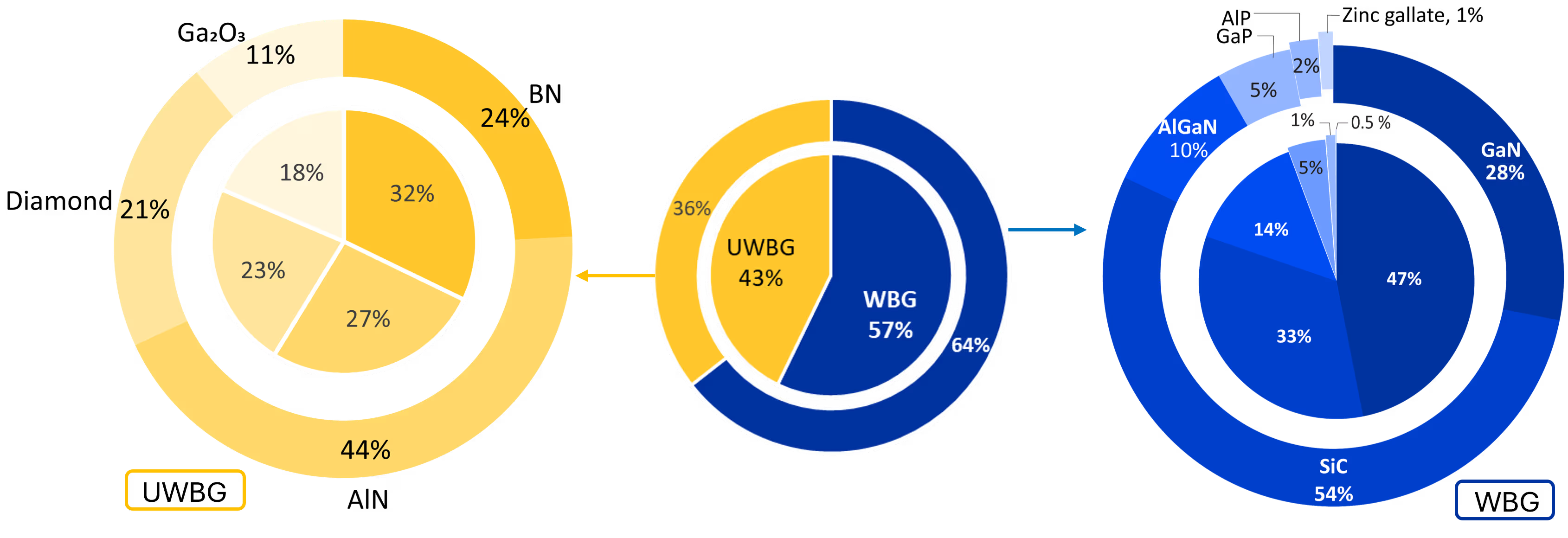
Within the WBG category (Figure 2 right), silicon carbide and gallium nitride dominate, but with notably different journal-patent dynamics. Silicon carbide exhibits a patent‑heavy profile, reflecting its industrial maturity and widespread commercialization in power electronics. Gallium nitride, by contrast, shows a more balanced journal‑to‑patent ratio, indicating active academic innovation alongside growing but less concentrated commercialization.
Additionally, AI and machine learning approaches are increasingly applied to mature WBG platforms such as silicon carbide and gallium nitride to support device modeling, defect analyses, and manufacturing yield optimization. In parallel, there’s a notable resurgence of interest in phosphide WBG materials, such as AlP and GaP, driven by revised hybrid-functional bandgap calculations that position them alongside traditional III–V semiconductors for future high-frequency and heterostructure applications.
On the UWBG side, the landscape is dominated by broad academic exploration, with significant journal activity in AlN, BN, diamond, and emerging materials like Ga2O3. Patent activity in UWBG materials is more focused, especially around AlN, which stands out as the most commercially promising candidate in this class. This is attributed to its thermal management properties bridging current market needs.
Collectively, these patterns reveal a technology pipeline in which silicon carbide and gallium nitride occupy the mature, deployment‑ready end of the spectrum, while UWBG materials remain research‑intensive but show early signs of industrial uptake, marking them as the next frontier for future extreme‑environment technologies.
Device landscape reveals the technology readiness level
To understand how these material trends translate into practical technology adoption, we used CAS-indexed concepts to map WBG and UWBG materials to specific device categories, from power electronics to radio frequency components.

The device distribution highlights how WBG and UWBG semiconductors concentrate around functions where their electrical, thermal, and optical advantages translate into performance gains (see Figure 3). Transistor technologies dominate because these materials enable voltage handling, switching speed, and heat tolerance far beyond what silicon can support. This is reflected in the strong activity across advanced transistor architectures, HEMTs, FinFETs, MISFETs, and HEFTs, which rely on high breakdown fields and fast carrier transport to deliver efficient high-power and high-frequency operations. Light-emitting devices form the next major cluster, in which wide bandgaps allow efficient photon generation across a broad spectrum, supporting LEDs, microLED displays, semiconductor lasers, and UV emitters used in communication, sensing, and sterilization.
Beyond these dominant device families, the spread into integrated circuits (ICs), memory elements, thermal-management components, energy-storage interfaces, and sensing layers shows how the stability, high-field tolerance, and chemical robustness of WBG/UWBG materials enable electronics to function reliably in high heat, voltage, and radiation conditions, as well as corrosive environments that push beyond silicon’s operating envelope.
Recent innovations describe amorphous silicon carbide combined with nano‑silicon and hydrocarbon phases to create compressive, mechanically resilient electrode frameworks that suppress volume expansion and improve cycling stability and rate performance. Silicon carbide and boron nitride also feature prominently in thermal‑management components, particularly for EV battery modules, where their high thermal conductivity, electrical insulation, and extreme temperature stability enable efficient heat spreading and robust structural performance.
Patents show their use in ceramic coatings, vapor-chamber interfaces, and heat-dissipating layers designed to maintain safe, compact battery-pack operation. In gas-sensing applications, WBG/UWBG oxides and nitrides, including AlN, Ga2O3, and GaN, provide chemically stable, high-bandgap barrier layers that support electron-tunneling detection and selective chemisorption. Developments include conformal UWBG coatings over porous sensing films to achieve drift-resistant, high-accuracy miniature gas sensors suitable for harsh environments.
Emerging device applications for wide bandgap semiconductors
While the device landscape describes how WBG and UWBG materials are distributed across device categories, examining devices through their average growth rates in recent years (2023-2025) offers a complementary view on research and patent activity.
The emerging device landscape reveals how WBG and UWBG materials are extending innovation into new regimes that were previously inaccessible (see Figure 4). One striking observation is the association of silicon carbide with femtosecond laser‑related device activity. Although silicon carbide is an indirect bandgap material and not suitable as a traditional laser medium, this link reflects rapid progress in femtosecond laser‑based color‑center engineering, where researchers can now write quantum defects inside silicon carbide with high spatial precision. This is an emerging capability known as quantum defect engineering that is unlocking new quantum photonics and sensing platforms.
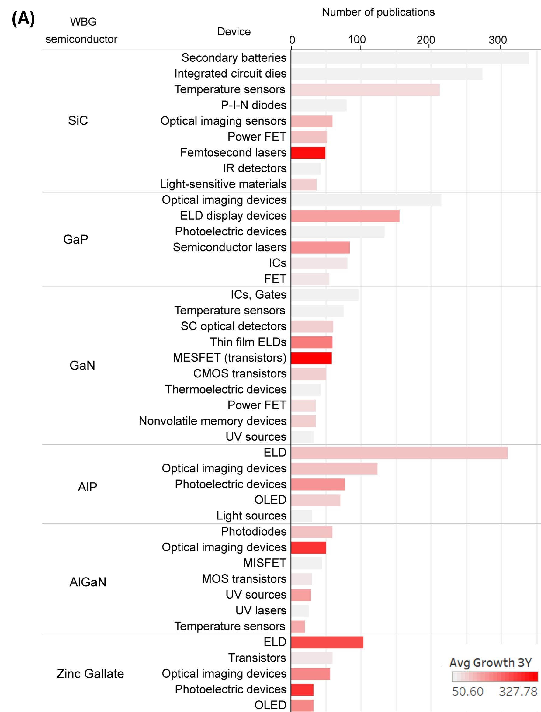
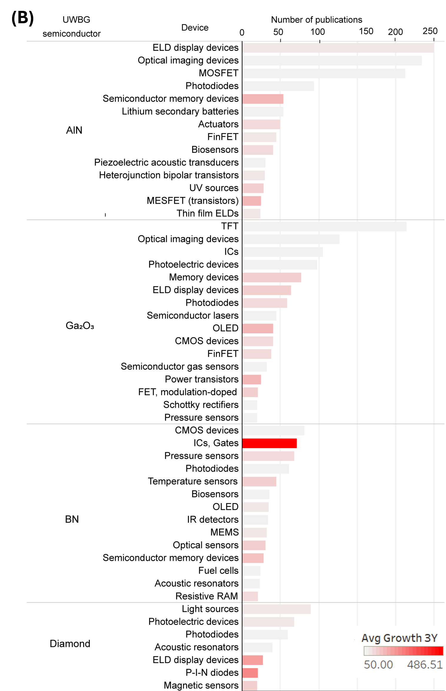
Another prominent observation is the growing appearance of boron nitride in IC‑ and gate‑related categories. Boron nitride is not an active semiconductor for logic applications. Instead, it is becoming a vital interface engineering and insulating/dielectric material in advanced transistor architectures. Its atomically flat surface, UBG, and chemically inert nature make boron nitride indispensable for 2D FETs, gate dielectrics, barrier layers, and nanoscale IC layouts, which explains its sharp rise in publications tied to ICs and gate structures.
Gallium nitride’s association with MESFETs aligns with its established role as an active semiconductor channel in these devices. Its wide bandgap ensures low leakage and high breakdown voltages, while high electron mobility and saturation velocity support efficient high‑frequency and high‑power operations. These properties make gallium nitride MESFETs well suited for fast switching and radio frequency (RF) applications.
More broadly, gallium nitride and Ga2O3 cluster around high‑power and high‑frequency device categories, reflecting intensifying demand for components capable of operating reliably under extreme thermal and electrical conditions. In contrast, GaP, AlN, and zinc gallate anchor rapidly expanding optoelectronic domains — from UV emission to advanced sensing and display technologies — while AlP appears as a small‑volume but strategically emerging material linked to next‑generation photodetectors, memory devices, and UV sources.
Overall, the landscape of emerging devices underscores how intrinsic material advantages are steering innovation across power electronics, photonics, and new nanoscale device platforms.
How devices translate to applications of wide bandgap semiconductors
We can get a sense of the major application categories for WBG and UWBG semiconductors through the device landscape. By examining overall publication volume and journal‑to‑patent ratios, however, we can identify which fields show stronger commercial pulls and which remain more research‑leaning within the broader innovation spectrum.

The application landscape shows optoelectronics and power electronics as the most publication‑dense domains, with near‑balanced journal-to-patent (J/P) ratios (≈1.0) reflecting strong academic research supported by active patenting across GaN/AlGaN‑based LEDs, UV emitters, laser architectures, SiC MOSFETs, and GaN HEMTs (see Figure 5A). Communication and sensing applications fall into a mid‑range J/P zone (≈0.7–0.8), indicating steady academic interest with more selective, early‑stage patenting as materials like GaN, AlN, and Ga2O3 enable stable, high‑accuracy RF and gas‑sensing platforms under harsh conditions.
Energy‑storage and conversion systems show the lowest J/P ratios (≈0.18), pointing to a patent‑driven profile where innovations such as silicon carbide‑reinforced anodes, boron nitride and Ga2O3 interfacial engineering, and diamond‑based electrode architectures are advanced through targeted industrial development despite lower overall publication volumes.
Optoelectronics
WBG/UWBG materials now anchor the optoelectronics stack from deep‑UV to near‑IR, with gallium nitride and silicon carbide leading publication volumes and AlN, BN, diamond, and Ga2O3 expanding capability into the UV‑C and harsh‑environment regimes (see Figure 5B). Gallium nitride and AlGaN underpin high‑efficiency LEDs, micro‑LEDs, lasers, and visible‑light communication (VLC), while silicon carbide provides thermally robust substrates and co‑integration pathways for high‑power emitters and RF front‑ends.
On the ultra-wide-bandgap frontier, AlN and boron nitride (including h-BN) enable solar-blind photodetectors and deep-UV emitters. Diamond contributes extreme thermal conductivity and quantum-photonics functionality, and Ga2O3 pushes power handling and UV detection via its high breakdown field. Around these materials, the patent corpus reveals accelerating progress in epitaxy, polarity control, nanostructuring, surface passivation, and singulation. This kind of process innovation turns lab-scale breakthroughs into scalable devices.
The device space reflects this: micro-LEDs and quantum-dot color conversion for advanced displays; III-N lasers and VCSEL-class architectures for compact, efficient light sources; and emerging superconducting-semiconducting hybrids for single-photon detection, where WBGs such as silicon carbide are used as substrate to withstand high critical temperature.
This trajectory is tightly coupled to industries where leading companies convert WBG/UWBG science into manufacturing-ready platforms. Device makers such as Samsung, Sony, AMS OSRAM, TCL Technology, and Mitsubishi Electric dominate patents in LEDs, micro-LED displays, lasers, and imaging systems. This aligns with the GaN/AlGaN publication dominance and pushes toward finer pixels, higher brightness, and better color conversion. Disco and Applied Materials contribute the enabling infrastructure, such as laser dicing, wafer thinning, bonding, surface treatment, and die-level handling, needed to process brittle, thermally demanding WBG/UWBG wafers at volume.
Foundries and integrators (e.g., TSMC, Intel) extend the stack with silicon photonics, III‑N RF integration, and back‑end packaging flows, while specialized silicon carbide and gallium nitride materials providers stabilize the substrate and epitaxy supply chain. This creates a self‑reinforcing cycle: advances in materials unlock new device concepts, which in turn drive patents in manufacturability and yield‑critical steps, thereby propelling the industry toward increasingly mature, scalable WBG/UWBG technology platforms.
Power electronics
The patent landscape reveals a power electronics ecosystem undergoing rapid maturation, driven predominantly by silicon carbide and gallium nitride (see Figure 5B). Silicon carbide stands out as the central pillar, with numerous patents on silicon carbide semiconductor devices, epitaxial wafer technologies, and high‑voltage modules designed for electric vehicles, industrial drives, and railway power systems. Its high thermal conductivity, wide bandgap, and breakdown strength make silicon carbide the material of choice for traction inverters, onboard chargers, and high‑efficiency power conversion circuits.
Gallium nitride, meanwhile, is increasingly integrated for high‑frequency and high‑power switching, with patents describing advanced HEMTs and gallium nitride layers grown over silicon carbide substrates to unlock higher power densities. Together, silicon carbide and gallium nitride form the technological backbone of modern power conversion, each reinforcing the other’s performance envelope.
Across applications, transportation and industrial power conversion dominate, with nearly one-third of patents tied to EV traction systems, mobility control, and heavy-duty automation. Power-conversion and management filings are even more prominent, emphasizing thermal-resistance reduction, advanced AlN packaging, and reliability-driven module design. A consistent theme is that WBG materials alone are insufficient. Packaging, thermomechanical design, and system-level integration must advance in parallel. Many patents focus on supporting infrastructure, including epitaxy control, defect management, wafer thinning, bonding, and specialized RF or sensing modules.
Sensing
In sensing applications, WBG/UWBG oxides and nitrides provide chemically stable, high-bandgap barrier layers supporting electron-tunneling detection and selective chemisorption. Patents focused on advanced doping and lattice engineering demonstrate efforts to create reliably doped gallium nitride AlN, and Ga2O3 materials with controlled p‑ and n‑type regions, improving sensitivity and robustness for high‑temperature pressure, gas, and chemical sensors. These materials’ high breakdown fields and wide bandgaps support deep‑UV photodetectors, RF/microwave sensing, and extreme‑environment sensor electronics, aligning with broader technology development goals highlighted in programs such as DARPA’s UWBG initiative targeting advanced sensor‑grade AlN, c‑BN, and diamond.
Communication
Materials such as gallium nitride, AlN, and SiC now anchor advanced RF communication technologies for 5G, 6G, Wi‑Fi 6E, and emerging sub‑THz systems. Patents heavily focus on high‑efficiency RF power amplifiers and front‑end modules, with gallium nitride favored for its high electron mobility, breakdown strength, and excellent high‑frequency performance. Key innovations include gallium nitride HEMTs, co‑integrated power amplifiers with on‑chip voltage regulation, and multiband front‑end circuits tailored for massive multiple input multiple output (MIMO), millimeter-wave (mmWave) access points, and satellite terminals. AlN‑based Film bulk acoustic resonator (FBAR) and Surface acoustic wave (SAW) resonators remain essential for 5G mid‑band and Wi‑Fi coexistence, leveraging high acoustic velocity and high‑Q materials for low loss and stable filtering at increasingly high frequencies.
エネルギー貯蔵
エネルギー貯蔵分野における論文数に対する特許数の比率は約0.18と最も低く、特許主導の開発が進んでいることを示しています。炭化ケイ素強化アノード、窒化ホウ素界面エンジニアリング、ダイヤモンドベースの電極構造などが、ターゲットを絞った産業開発を通じて進化しています。近年の特許では、アモルファス炭化ケイ素とナノシリコンを組み合わせることで、体積膨張を抑制しサイクル安定性を向上させる、機械的に強靭な電極フレームワークが提案されています。炭化ケイ素と窒化ホウ素は、EVバッテリーモジュールの熱管理コンポーネントにおいて重要な役割を担っており、その高い熱伝導率と極限環境下での安定性により、効率的な放熱を実現しています。
ワイドバンドギャップ半導体技術の未来
WBG(ワイドバンドギャップ)およびUWBG(超ワイドバンドギャップ)半導体の軌跡は、今後10年間、性能と商用化の両面で継続的な成長が見込まれることを示しています。炭化ケイ素は、電動化された輸送機器、再生可能エネルギーシステム、産業オートメーションにおいて、より高い耐電圧性、熱的堅牢性、長期信頼性が求められる中、高電力変換の基盤であり続けるでしょう。一方、窒化ガリウムは、急速充電用パワーエレクトロニクス、RFフロントエンド、ミリ波システム、そして新たに登場したサブテラヘルツ通信へとその領域を拡大しています。
AlN、Ga2O3、BN、ダイヤモンドといったUWBG材料は、深紫外フォトニクス、極限環境センシング、超高電圧スイッチング、高度な誘電体および量子デバイスインターフェースといった次なるフロンティアを切り拓くと期待されています。特に、ドーピング、エピタキシャル成長、欠陥エンジニアリングにおける課題が克服されつつあることが、その進展を後押ししています。
あらゆる材料クラスにおいて、今後の採用を決定づける要因は、熱管理、異種材料集積、そしてスケーラブルな製造技術となります。性能がパッケージング、界面エンジニアリング、モジュールレベルの共同設計に依存するようになるにつれ、競争優位性は、材料イノベーションと信頼性の高い大量生産技術を融合できる企業へとシフトしていくでしょう。
今後の展望として、WBGおよびUWBG半導体は、次世代のエネルギー、通信、モビリティ、センシング技術を支える基盤となり、より電化され、接続され、高周波化する世界の核心的な構成要素となるでしょう。