
.avif)

Executive Summary
- Wide bandgap and ultra-wide bandgap semiconductors can achieve superior electrical and thermal performance over standard silicon semiconductors because the energy separation between bands supports high-temperature, high-power applications.
- Silicon carbide and gallium nitride are the most-researched materials for these semiconductors, with silicon carbide more common in patent literature.
- The leading devices using wide bandgap and ultra-wide bandgap semiconductors are transistors, light emitters, and integrated circuits/memory devices, demonstrating the need for semiconductors capable of handling high-intensity environments.
- Optoelectronics and power electronics are the primary applications for wide bandgap and ultra-wide bandgap materials.
Semiconductor applications span an extraordinary range — from milliwatt mobile chargers to gigawatt industrial systems, and high-precision sensors to advanced optoelectronic devices. For decades, silicon (Si) has been the cornerstone of semiconductor technology, enabling countless innovations across industries. However, as performance demands escalate across multiple application domains, silicon’s fundamental material properties, such as a relatively small bandgap and limited thermal handling, have become a limiting factor in high-voltage, high-temperature, and high-power applications.
The solution lies in wide bandgap (WBG) and ultra-wide bandgap (UWBG) semiconductors. These advanced materials possess a larger energy gap between their valence and conduction bands compared to silicon, unlocking superior performance characteristics. This drives numerous performance advantages across demanding, high-stress environments.
What are wide and ultra-wide bandgap semiconductors?
Wide‑bandgap and ultra‑wide bandgap materials achieve superior performance because their wider bandgaps stem from stronger, shorter, and more ionic or covalent bonds, such as C–C in diamond or Al–N and Ga–N in III-N semiconductors. This localizes electrons and reduces orbital overlap, creating large energy separation between bands. These stiff bonding networks, often involving light atoms like C, N, and B, produce high phonon energies and excellent thermal conductivity, enabling high‑temperature and high‑power operation.
WBG materials have a bandgap typically in the range of 2–4 eV, significantly larger than that of silicon (~1.2 eV). Key materials include silicon carbide (SiC,~3.2 eV) and gallium nitride (GaN, ~3.4 eV), which are widely used in high-voltage, high-temperature, and high-frequency power and radio frequency (RF) devices. UWBG materials take performance even further with bandgaps > 4 eV, offering dramatic improvements over silicon and WBG materials. This includes materials such as gallium oxide (β‑ Ga2O3, ~4.8 eV), aluminum nitride (AlN, ~6.2 eV) and cubic boron nitride (c‑BN, ~6.4 eV). UWBGs also offer enhancements in breakdown strength, power density, and extreme environment capability.
Data-driven analyses can help us examine the fundamental drivers behind the WBG semiconductor transition. It also lets us explore its transformative implications across power electronics and optoelectronic and sensing applications. Using a focused search strategy built from selected CAS Registry Numbers® and application-specific CAS-controlled terms, we identified over 77,000 journal articles and patent families from the CAS Content Collection™ via CAS IP Finder, powered by STNTM.

The data shows that WBG and UWBG semiconductors are a rapidly advancing, commercially relevant technology space characterized by accelerated scientific output and strong commercialization trends. Publication trends from 2016-2025 show a sustained upward trajectory, with marked acceleration after 2019 and peak activity by 2025: clear signals that the field is transitioning from exploratory research into technological maturity. Patents outpacing journal publications underscore this shift. The industry is no longer observing, but protecting IP, scaling innovations, and pushing devices toward market integration.
Silicon carbide and gallium nitride dominate the material landscape
The relative contribution of journals and patents within each material category in Figure 2 (central chart), shows that journal publications are relatively balanced between WBG (57%) and UWBG (43%), whereas patent activity leans more toward WBG materials (64% WBG vs. 36% UWBG). This contrast indicates that while WBG materials are already translating into commercial technologies, UWBG materials remain largely research-driven, with broader commercialization expected to follow as technical maturity and industrial confidence increase.
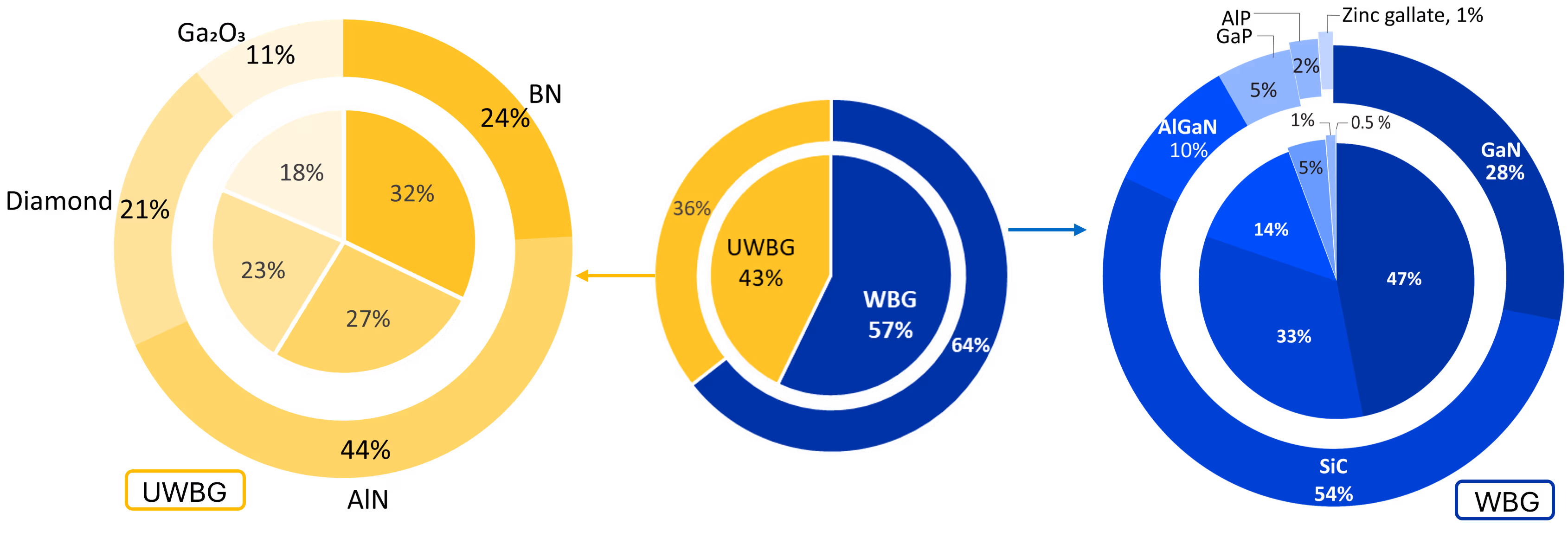
Within the WBG category (Figure 2 right), silicon carbide and gallium nitride dominate, but with notably different journal-patent dynamics. Silicon carbide exhibits a patent‑heavy profile, reflecting its industrial maturity and widespread commercialization in power electronics. Gallium nitride, by contrast, shows a more balanced journal‑to‑patent ratio, indicating active academic innovation alongside growing but less concentrated commercialization.
Additionally, AI and machine learning approaches are increasingly applied to mature WBG platforms such as silicon carbide and gallium nitride to support device modeling, defect analyses, and manufacturing yield optimization. In parallel, there’s a notable resurgence of interest in phosphide WBG materials, such as AlP and GaP, driven by revised hybrid-functional bandgap calculations that position them alongside traditional III–V semiconductors for future high-frequency and heterostructure applications.
On the UWBG side, the landscape is dominated by broad academic exploration, with significant journal activity in AlN, BN, diamond, and emerging materials like Ga2O3. Patent activity in UWBG materials is more focused, especially around AlN, which stands out as the most commercially promising candidate in this class. This is attributed to its thermal management properties bridging current market needs.
Collectively, these patterns reveal a technology pipeline in which silicon carbide and gallium nitride occupy the mature, deployment‑ready end of the spectrum, while UWBG materials remain research‑intensive but show early signs of industrial uptake, marking them as the next frontier for future extreme‑environment technologies.
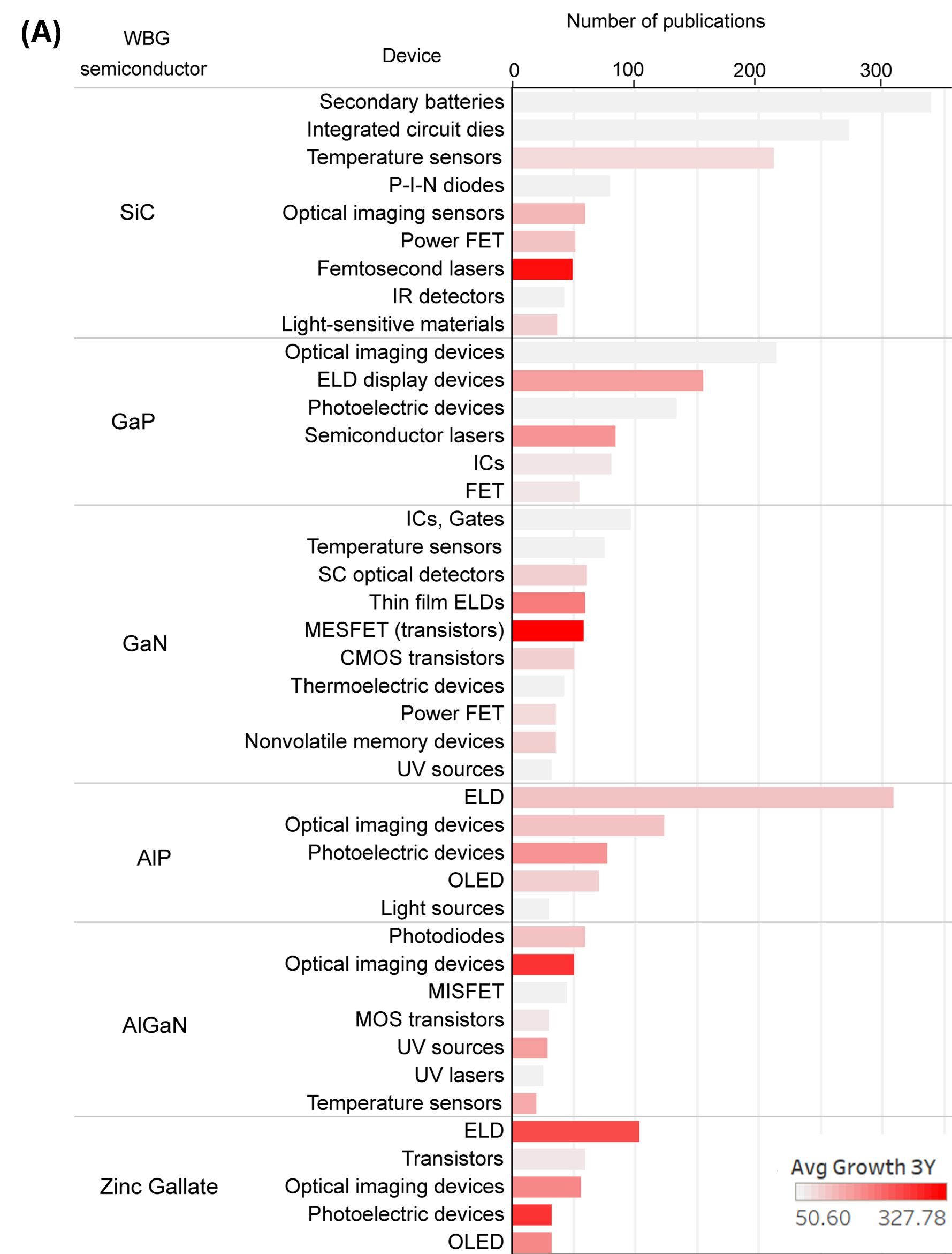
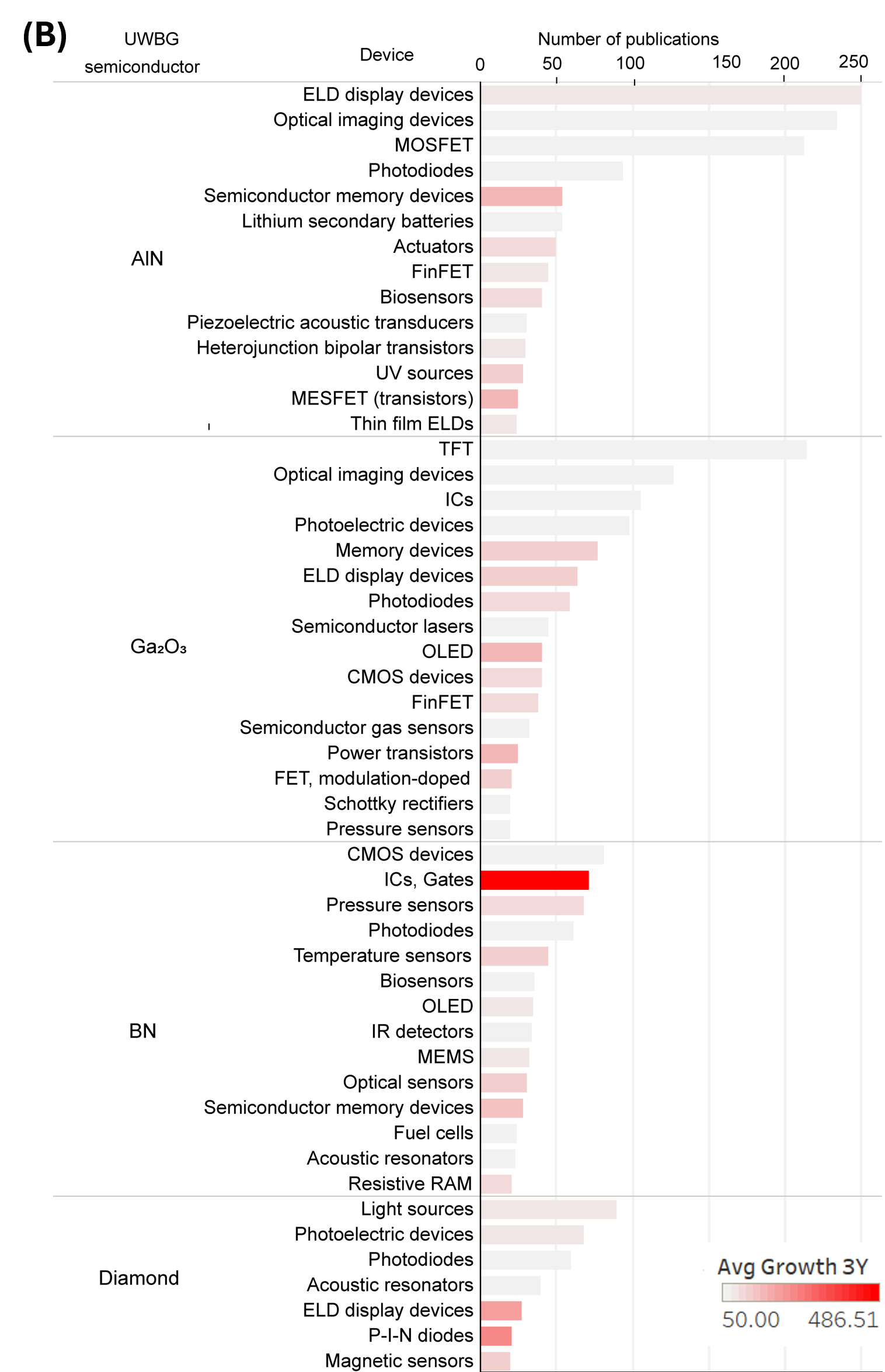
Device landscape reveals the technology readiness level
To understand how these material trends translate into practical technology adoption, we used CAS-indexed concepts to map WBG and UWBG materials to specific device categories, from power electronics to radio frequency components.

The device distribution highlights how WBG and UWBG semiconductors concentrate around functions where their electrical, thermal, and optical advantages translate into performance gains (see Figure 3). Transistor technologies dominate because these materials enable voltage handling, switching speed, and heat tolerance far beyond what silicon can support. This is reflected in the strong activity across advanced transistor architectures, HEMTs, FinFETs, MISFETs, and HEFTs, which rely on high breakdown fields and fast carrier transport to deliver efficient high-power and high-frequency operations. Light-emitting devices form the next major cluster, in which wide bandgaps allow efficient photon generation across a broad spectrum, supporting LEDs, microLED displays, semiconductor lasers, and UV emitters used in communication, sensing, and sterilization.
Beyond these dominant device families, the spread into integrated circuits (ICs), memory elements, thermal-management components, energy-storage interfaces, and sensing layers shows how the stability, high-field tolerance, and chemical robustness of WBG/UWBG materials enable electronics to function reliably in high heat, voltage, and radiation conditions, as well as corrosive environments that push beyond silicon’s operating envelope.
Recent innovations describe amorphous silicon carbide combined with nano‑silicon and hydrocarbon phases to create compressive, mechanically resilient electrode frameworks that suppress volume expansion and improve cycling stability and rate performance. Silicon carbide and boron nitride also feature prominently in thermal‑management components, particularly for EV battery modules, where their high thermal conductivity, electrical insulation, and extreme temperature stability enable efficient heat spreading and robust structural performance.
Patents show their use in ceramic coatings, vapor-chamber interfaces, and heat-dissipating layers designed to maintain safe, compact battery-pack operation. In gas-sensing applications, WBG/UWBG oxides and nitrides, including AlN, Ga2O3, and GaN, provide chemically stable, high-bandgap barrier layers that support electron-tunneling detection and selective chemisorption. Developments include conformal UWBG coatings over porous sensing films to achieve drift-resistant, high-accuracy miniature gas sensors suitable for harsh environments.
Emerging device applications for wide bandgap semiconductors
While the device landscape describes how WBG and UWBG materials are distributed across device categories, examining devices through their average growth rates in recent years (2023-2025) offers a complementary view on research and patent activity.
The emerging device landscape reveals how WBG and UWBG materials are extending innovation into new regimes that were previously inaccessible (see Figure 4). One striking observation is the association of silicon carbide with femtosecond laser‑related device activity. Although silicon carbide is an indirect bandgap material and not suitable as a traditional laser medium, this link reflects rapid progress in femtosecond laser‑based color‑center engineering, where researchers can now write quantum defects inside silicon carbide with high spatial precision. This is an emerging capability known as quantum defect engineering that is unlocking new quantum photonics and sensing platforms.
Another prominent observation is the growing appearance of boron nitride in IC‑ and gate‑related categories. Boron nitride is not an active semiconductor for logic applications. Instead, it is becoming a vital interface engineering and insulating/dielectric material in advanced transistor architectures. Its atomically flat surface, UBG, and chemically inert nature make boron nitride indispensable for 2D FETs, gate dielectrics, barrier layers, and nanoscale IC layouts, which explains its sharp rise in publications tied to ICs and gate structures.
Gallium nitride’s association with MESFETs aligns with its established role as an active semiconductor channel in these devices. Its wide bandgap ensures low leakage and high breakdown voltages, while high electron mobility and saturation velocity support efficient high‑frequency and high‑power operations. These properties make gallium nitride MESFETs well suited for fast switching and radio frequency (RF) applications.
More broadly, gallium nitride and Ga2O3 cluster around high‑power and high‑frequency device categories, reflecting intensifying demand for components capable of operating reliably under extreme thermal and electrical conditions. In contrast, GaP, AlN, and zinc gallate anchor rapidly expanding optoelectronic domains — from UV emission to advanced sensing and display technologies — while AlP appears as a small‑volume but strategically emerging material linked to next‑generation photodetectors, memory devices, and UV sources.
Overall, the landscape of emerging devices underscores how intrinsic material advantages are steering innovation across power electronics, photonics, and new nanoscale device platforms.
How devices translate to applications of wide bandgap semiconductors
We can get a sense of the major application categories for WBG and UWBG semiconductors through the device landscape. By examining overall publication volume and journal‑to‑patent ratios, however, we can identify which fields show stronger commercial pulls and which remain more research‑leaning within the broader innovation spectrum.

The application landscape shows optoelectronics and power electronics as the most publication‑dense domains, with near‑balanced journal-to-patent (J/P) ratios (≈1.0) reflecting strong academic research supported by active patenting across GaN/AlGaN‑based LEDs, UV emitters, laser architectures, SiC MOSFETs, and GaN HEMTs (see Figure 5A). Communication and sensing applications fall into a mid‑range J/P zone (≈0.7–0.8), indicating steady academic interest with more selective, early‑stage patenting as materials like GaN, AlN, and Ga2O3 enable stable, high‑accuracy RF and gas‑sensing platforms under harsh conditions.
Energy‑storage and conversion systems show the lowest J/P ratios (≈0.18), pointing to a patent‑driven profile where innovations such as silicon carbide‑reinforced anodes, boron nitride and Ga2O3 interfacial engineering, and diamond‑based electrode architectures are advanced through targeted industrial development despite lower overall publication volumes.
Optoelectronics
WBG/UWBG materials now anchor the optoelectronics stack from deep‑UV to near‑IR, with gallium nitride and silicon carbide leading publication volumes and AlN, BN, diamond, and Ga2O3 expanding capability into the UV‑C and harsh‑environment regimes (see Figure 5B). Gallium nitride and AlGaN underpin high‑efficiency LEDs, micro‑LEDs, lasers, and visible‑light communication (VLC), while silicon carbide provides thermally robust substrates and co‑integration pathways for high‑power emitters and RF front‑ends.
On the ultra-wide-bandgap frontier, AlN and boron nitride (including h-BN) enable solar-blind photodetectors and deep-UV emitters. Diamond contributes extreme thermal conductivity and quantum-photonics functionality, and Ga2O3 pushes power handling and UV detection via its high breakdown field. Around these materials, the patent corpus reveals accelerating progress in epitaxy, polarity control, nanostructuring, surface passivation, and singulation. This kind of process innovation turns lab-scale breakthroughs into scalable devices.
The device space reflects this: micro-LEDs and quantum-dot color conversion for advanced displays; III-N lasers and VCSEL-class architectures for compact, efficient light sources; and emerging superconducting-semiconducting hybrids for single-photon detection, where WBGs such as silicon carbide are used as substrate to withstand high critical temperature.
This trajectory is tightly coupled to industries where leading companies convert WBG/UWBG science into manufacturing-ready platforms. Device makers such as Samsung, Sony, AMS OSRAM, TCL Technology, and Mitsubishi Electric dominate patents in LEDs, micro-LED displays, lasers, and imaging systems. This aligns with the GaN/AlGaN publication dominance and pushes toward finer pixels, higher brightness, and better color conversion. Disco and Applied Materials contribute the enabling infrastructure, such as laser dicing, wafer thinning, bonding, surface treatment, and die-level handling, needed to process brittle, thermally demanding WBG/UWBG wafers at volume.
Foundries and integrators (e.g., TSMC, Intel) extend the stack with silicon photonics, III‑N RF integration, and back‑end packaging flows, while specialized silicon carbide and gallium nitride materials providers stabilize the substrate and epitaxy supply chain. This creates a self‑reinforcing cycle: advances in materials unlock new device concepts, which in turn drive patents in manufacturability and yield‑critical steps, thereby propelling the industry toward increasingly mature, scalable WBG/UWBG technology platforms.
Power electronics
The patent landscape reveals a power electronics ecosystem undergoing rapid maturation, driven predominantly by silicon carbide and gallium nitride (see Figure 5B). Silicon carbide stands out as the central pillar, with numerous patents on silicon carbide semiconductor devices, epitaxial wafer technologies, and high‑voltage modules designed for electric vehicles, industrial drives, and railway power systems. Its high thermal conductivity, wide bandgap, and breakdown strength make silicon carbide the material of choice for traction inverters, onboard chargers, and high‑efficiency power conversion circuits.
Gallium nitride, meanwhile, is increasingly integrated for high‑frequency and high‑power switching, with patents describing advanced HEMTs and gallium nitride layers grown over silicon carbide substrates to unlock higher power densities. Together, silicon carbide and gallium nitride form the technological backbone of modern power conversion, each reinforcing the other’s performance envelope.
Across applications, transportation and industrial power conversion dominate, with nearly one-third of patents tied to EV traction systems, mobility control, and heavy-duty automation. Power-conversion and management filings are even more prominent, emphasizing thermal-resistance reduction, advanced AlN packaging, and reliability-driven module design. A consistent theme is that WBG materials alone are insufficient. Packaging, thermomechanical design, and system-level integration must advance in parallel. Many patents focus on supporting infrastructure, including epitaxy control, defect management, wafer thinning, bonding, and specialized RF or sensing modules.
Sensing
In sensing applications, WBG/UWBG oxides and nitrides provide chemically stable, high-bandgap barrier layers supporting electron-tunneling detection and selective chemisorption. Patents focused on advanced doping and lattice engineering demonstrate efforts to create reliably doped gallium nitride AlN, and Ga2O3 materials with controlled p‑ and n‑type regions, improving sensitivity and robustness for high‑temperature pressure, gas, and chemical sensors. These materials’ high breakdown fields and wide bandgaps support deep‑UV photodetectors, RF/microwave sensing, and extreme‑environment sensor electronics, aligning with broader technology development goals highlighted in programs such as DARPA’s UWBG initiative targeting advanced sensor‑grade AlN, c‑BN, and diamond.
Communication
Materials such as gallium nitride, AlN, and SiC now anchor advanced RF communication technologies for 5G, 6G, Wi‑Fi 6E, and emerging sub‑THz systems. Patents heavily focus on high‑efficiency RF power amplifiers and front‑end modules, with gallium nitride favored for its high electron mobility, breakdown strength, and excellent high‑frequency performance. Key innovations include gallium nitride HEMTs, co‑integrated power amplifiers with on‑chip voltage regulation, and multiband front‑end circuits tailored for massive multiple input multiple output (MIMO), millimeter-wave (mmWave) access points, and satellite terminals. AlN‑based Film bulk acoustic resonator (FBAR) and Surface acoustic wave (SAW) resonators remain essential for 5G mid‑band and Wi‑Fi coexistence, leveraging high acoustic velocity and high‑Q materials for low loss and stable filtering at increasingly high frequencies.
Energy storage
Energy storage applications show the lowest journal-to-patent ratios (~0.18), indicating patent-driven development where silicon carbide-reinforced anodes, boron nitride interfacial engineering, and diamond-based electrode architectures advance through targeted industrial development. Recent patents describe amorphous silicon carbide combined with nano-silicon to create mechanically resilient electrode frameworks that suppress volume expansion and improve cycling stability. Silicon carbide and boron nitride feature prominently in thermal-management components for EV battery modules, where their high thermal conductivity and extreme temperature stability enable efficient heat spreading.
The future of wide bandgap semiconductor technology
The trajectory of WBG and UWBG semiconductors points toward a decade of continued growth in capabilities and commercialization. Silicon carbide is poised to remain the foundation of high-power conversion as electrified transportation, renewable-energy systems, and industrial automation demand higher voltage tolerance, thermal robustness, and long-term reliability. Meanwhile, gallium nitride is expanding its footprint across fast-charging power electronics, RF front ends, mmWave systems, and emerging sub-terahertz communication.
UWBG materials such as AlN, Ga2O3, BN, and diamond are expected to open the next frontier: deep-UV photonics, extreme-environment sensing, ultra-high-voltage switching, and advanced dielectric and quantum-device interfaces especially as doping, epitaxy, and defect-engineering challenges continue to be overcome.
Across all material classes, the decisive factors shaping future adoption will be thermal management, heterogeneous integration, and scalable manufacturing. As performance hinges more on packaging, interface engineering, and module-level co-design, the competitive edge will shift toward companies that can unite materials innovation with reliable, high-volume fabrication.
The outlook indicates that WBG and UWBG semiconductors will underpin the next generation of energy, communication, mobility, and sensing technologies, serving as the core building blocks of a more electrified, connected, and high-frequency world.


