
.avif)

执行摘要
- 宽禁带和超宽禁带半导体之所以能实现优于标准硅半导体的电气和热性能,是因为其能带间的能量间隙支持高温、高功率的应用。
- 碳化硅和氮化镓是目前研究最广泛的半导体材料,其中碳化硅在专利文献中更为常见。
- 宽禁带和超宽禁带半导体的主要应用器件包括晶体管、发光器件以及集成电路/存储设备,这充分证明了市场对能够应对高强度环境的半导体的需求。
- 光电子和电力电子是宽禁带和超宽禁带材料的主要应用领域。
半导体应用范围极其广泛,从毫瓦级的移动充电器到吉瓦级的工业系统,从高精度传感器到先进的光电器件,无所不包。几十年来,硅(Si)一直是半导体技术的基石,推动了各行各业无数的创新。然而,随着多个应用领域对性能要求的不断提升,硅材料固有的物理特性(如相对较小的禁带宽度和有限的耐热性)已成为其在高电压、高温和高功率应用中的制约因素。
解决方案在于宽禁带(WBG)和超宽禁带(UWBG)半导体。与硅相比,这些先进材料在价带和导带之间拥有更大的能量间隙,从而释放出卓越的性能特征。这为各种高要求、高压力的应用环境带来了显著的性能优势。
材料研究人员可以使用 CAS SciFinder 搜索材料科学文献,识别支持创新的结构-性能关系和合成方法。
什么是宽禁带和超宽禁带半导体?
宽禁带和超宽禁带材料之所以能实现卓越性能,是因为其更宽的禁带源于更强、更短且离子性或共价性更强的化学键,例如金刚石中的C–C键,或III-N族半导体中的Al–N和Ga–N键。这些化学键使电子局部化并减少了轨道重叠,从而在能带之间形成了巨大的能量间隙。这些通常涉及碳、氮、硼等轻原子的坚固键合网络,产生了高声子能量和优异的导热性,从而实现了高温和高功率运行。
WBG材料的禁带宽度通常在2–4 eV范围内,远大于硅(约1.2 eV)。关键材料包括碳化硅(SiC,约3.2 eV)和氮化镓(GaN,约3.4 eV),它们被广泛应用于高电压、高温和高频功率及射频(RF)器件中。UWBG材料的禁带宽度大于4 eV,将性能提升到了新的高度,较硅和WBG材料有了显著改进。此类材料包括氧化镓(β‑ Ga2O3,约4.8 eV)、氮化铝(AlN,约6.2 eV)和立方氮化硼(c‑BN,约6.4 eV)。UWBG材料还在击穿强度、功率密度和极端环境适应能力方面提供了增强。
Data-driven analyses can help us examine the fundamental drivers behind the WBG semiconductor transition. It also lets us explore its transformative implications across power electronics and optoelectronic and sensing applications. Using a focused search strategy built from selected CAS Registry Numbers® and application-specific CAS-controlled terms, we identified over 77,000 journal articles and patent families from the CAS Content Collection™ via CAS IP Finder, powered by STNTM.

数据显示,WBG和UWBG半导体是一个快速发展且具有商业价值的技术领域,其特点是科研产出加速和商业化趋势强劲。2016年至2025年的出版趋势显示出持续上升的轨迹,在2019年后显著加速,并于2025年达到峰值:这些明确信号表明该领域正从探索性研究转向技术成熟期。专利数量超过期刊出版物进一步凸显了这一转变。行业已不再处于观望状态,而是在积极保护知识产权、扩大创新规模,并推动器件向市场化集成迈进。
碳化硅和氮化镓在材料领域占据主导地位
The relative contribution of journals and patents within each material category in Figure 2 (central chart), shows that journal publications are relatively balanced between WBG (57%) and UWBG (43%), whereas patent activity leans more toward WBG materials (64% WBG vs. 36% UWBG). This contrast indicates that while WBG materials are already translating into commercial technologies, UWBG materials remain largely research-driven, with broader commercialization expected to follow as technical maturity and industrial confidence increase.
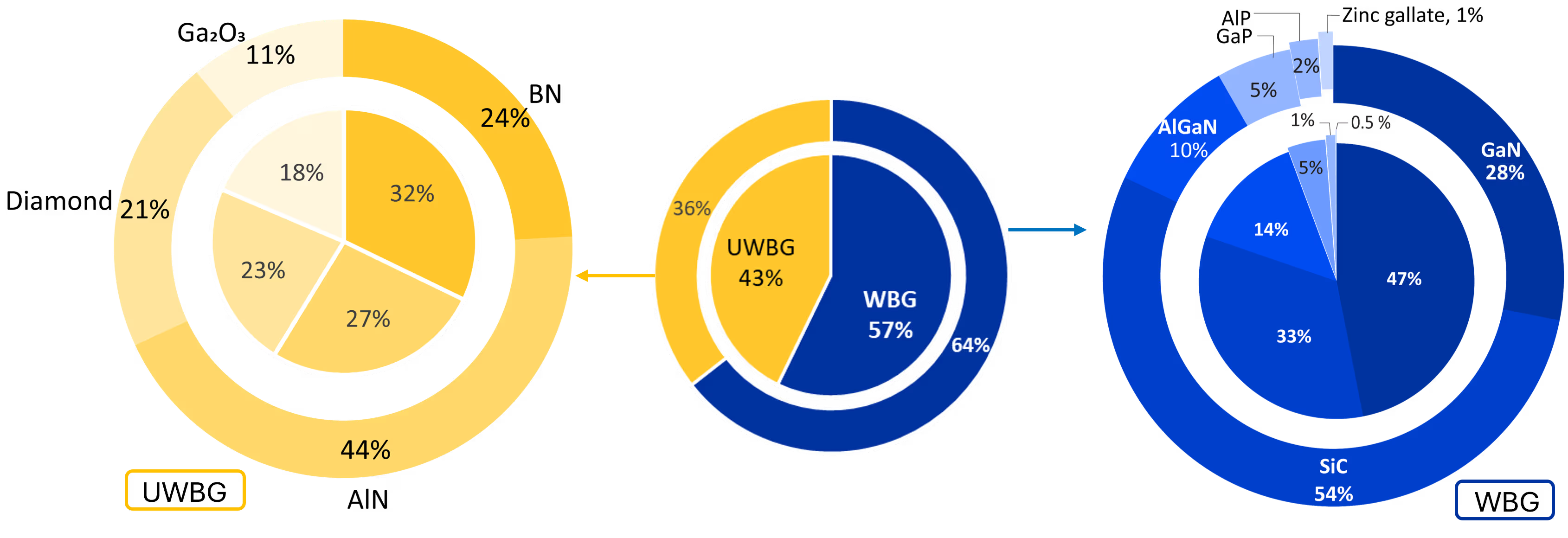
Within the WBG category (Figure 2 right), silicon carbide and gallium nitride dominate, but with notably different journal-patent dynamics. Silicon carbide exhibits a patent‑heavy profile, reflecting its industrial maturity and widespread commercialization in power electronics. Gallium nitride, by contrast, shows a more balanced journal‑to‑patent ratio, indicating active academic innovation alongside growing but less concentrated commercialization.
Additionally, AI and machine learning approaches are increasingly applied to mature WBG platforms such as silicon carbide and gallium nitride to support device modeling, defect analyses, and manufacturing yield optimization. In parallel, there’s a notable resurgence of interest in phosphide WBG materials, such as AlP and GaP, driven by revised hybrid-functional bandgap calculations that position them alongside traditional III–V semiconductors for future high-frequency and heterostructure applications.
On the UWBG side, the landscape is dominated by broad academic exploration, with significant journal activity in AlN, BN, diamond, and emerging materials like Ga2O3. Patent activity in UWBG materials is more focused, especially around AlN, which stands out as the most commercially promising candidate in this class. This is attributed to its thermal management properties bridging current market needs.
Collectively, these patterns reveal a technology pipeline in which silicon carbide and gallium nitride occupy the mature, deployment‑ready end of the spectrum, while UWBG materials remain research‑intensive but show early signs of industrial uptake, marking them as the next frontier for future extreme‑environment technologies.
Device landscape reveals the technology readiness level
To understand how these material trends translate into practical technology adoption, we used CAS-indexed concepts to map WBG and UWBG materials to specific device categories, from power electronics to radio frequency components.

The device distribution highlights how WBG and UWBG semiconductors concentrate around functions where their electrical, thermal, and optical advantages translate into performance gains (see Figure 3). Transistor technologies dominate because these materials enable voltage handling, switching speed, and heat tolerance far beyond what silicon can support. This is reflected in the strong activity across advanced transistor architectures, HEMTs, FinFETs, MISFETs, and HEFTs, which rely on high breakdown fields and fast carrier transport to deliver efficient high-power and high-frequency operations. Light-emitting devices form the next major cluster, in which wide bandgaps allow efficient photon generation across a broad spectrum, supporting LEDs, microLED displays, semiconductor lasers, and UV emitters used in communication, sensing, and sterilization.
Beyond these dominant device families, the spread into integrated circuits (ICs), memory elements, thermal-management components, energy-storage interfaces, and sensing layers shows how the stability, high-field tolerance, and chemical robustness of WBG/UWBG materials enable electronics to function reliably in high heat, voltage, and radiation conditions, as well as corrosive environments that push beyond silicon’s operating envelope.
Recent innovations describe amorphous silicon carbide combined with nano‑silicon and hydrocarbon phases to create compressive, mechanically resilient electrode frameworks that suppress volume expansion and improve cycling stability and rate performance. Silicon carbide and boron nitride also feature prominently in thermal‑management components, particularly for EV battery modules, where their high thermal conductivity, electrical insulation, and extreme temperature stability enable efficient heat spreading and robust structural performance.
Patents show their use in ceramic coatings, vapor-chamber interfaces, and heat-dissipating layers designed to maintain safe, compact battery-pack operation. In gas-sensing applications, WBG/UWBG oxides and nitrides, including AlN, Ga2O3, and GaN, provide chemically stable, high-bandgap barrier layers that support electron-tunneling detection and selective chemisorption. Developments include conformal UWBG coatings over porous sensing films to achieve drift-resistant, high-accuracy miniature gas sensors suitable for harsh environments.
Emerging device applications for wide bandgap semiconductors
While the device landscape describes how WBG and UWBG materials are distributed across device categories, examining devices through their average growth rates in recent years (2023-2025) offers a complementary view on research and patent activity.
The emerging device landscape reveals how WBG and UWBG materials are extending innovation into new regimes that were previously inaccessible (see Figure 4). One striking observation is the association of silicon carbide with femtosecond laser‑related device activity. Although silicon carbide is an indirect bandgap material and not suitable as a traditional laser medium, this link reflects rapid progress in femtosecond laser‑based color‑center engineering, where researchers can now write quantum defects inside silicon carbide with high spatial precision. This is an emerging capability known as quantum defect engineering that is unlocking new quantum photonics and sensing platforms.
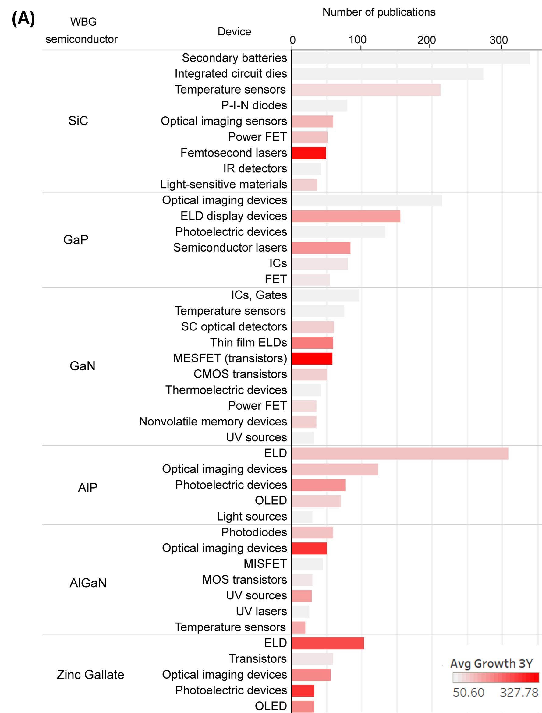
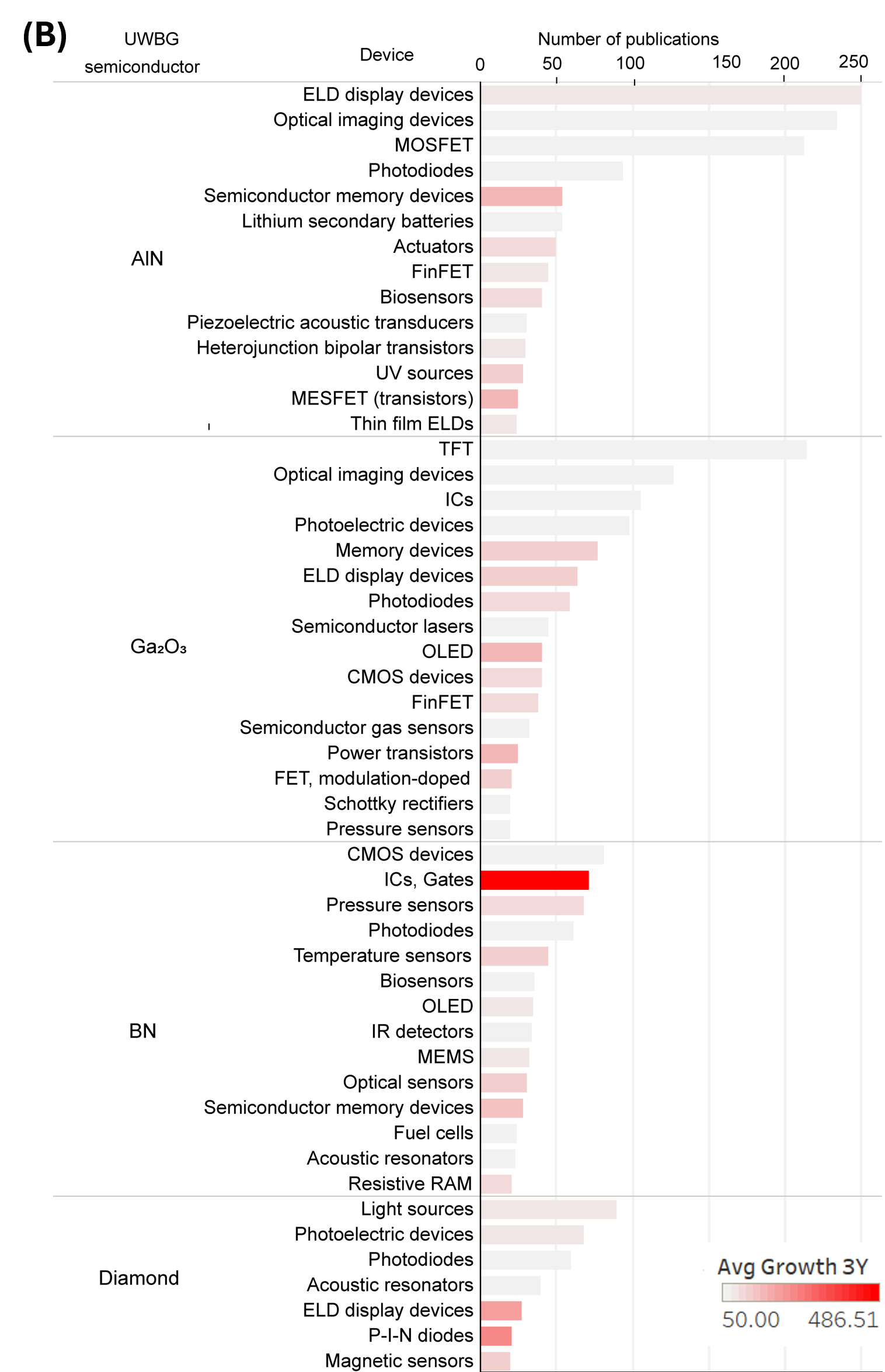
Another prominent observation is the growing appearance of boron nitride in IC‑ and gate‑related categories. Boron nitride is not an active semiconductor for logic applications. Instead, it is becoming a vital interface engineering and insulating/dielectric material in advanced transistor architectures. Its atomically flat surface, UBG, and chemically inert nature make boron nitride indispensable for 2D FETs, gate dielectrics, barrier layers, and nanoscale IC layouts, which explains its sharp rise in publications tied to ICs and gate structures.
Gallium nitride’s association with MESFETs aligns with its established role as an active semiconductor channel in these devices. Its wide bandgap ensures low leakage and high breakdown voltages, while high electron mobility and saturation velocity support efficient high‑frequency and high‑power operations. These properties make gallium nitride MESFETs well suited for fast switching and radio frequency (RF) applications.
More broadly, gallium nitride and Ga2O3 cluster around high‑power and high‑frequency device categories, reflecting intensifying demand for components capable of operating reliably under extreme thermal and electrical conditions. In contrast, GaP, AlN, and zinc gallate anchor rapidly expanding optoelectronic domains — from UV emission to advanced sensing and display technologies — while AlP appears as a small‑volume but strategically emerging material linked to next‑generation photodetectors, memory devices, and UV sources.
Overall, the landscape of emerging devices underscores how intrinsic material advantages are steering innovation across power electronics, photonics, and new nanoscale device platforms.
How devices translate to applications of wide bandgap semiconductors
We can get a sense of the major application categories for WBG and UWBG semiconductors through the device landscape. By examining overall publication volume and journal‑to‑patent ratios, however, we can identify which fields show stronger commercial pulls and which remain more research‑leaning within the broader innovation spectrum.

The application landscape shows optoelectronics and power electronics as the most publication‑dense domains, with near‑balanced journal-to-patent (J/P) ratios (≈1.0) reflecting strong academic research supported by active patenting across GaN/AlGaN‑based LEDs, UV emitters, laser architectures, SiC MOSFETs, and GaN HEMTs (see Figure 5A). Communication and sensing applications fall into a mid‑range J/P zone (≈0.7–0.8), indicating steady academic interest with more selective, early‑stage patenting as materials like GaN, AlN, and Ga2O3 enable stable, high‑accuracy RF and gas‑sensing platforms under harsh conditions.
Energy‑storage and conversion systems show the lowest J/P ratios (≈0.18), pointing to a patent‑driven profile where innovations such as silicon carbide‑reinforced anodes, boron nitride and Ga2O3 interfacial engineering, and diamond‑based electrode architectures are advanced through targeted industrial development despite lower overall publication volumes.
Optoelectronics
WBG/UWBG materials now anchor the optoelectronics stack from deep‑UV to near‑IR, with gallium nitride and silicon carbide leading publication volumes and AlN, BN, diamond, and Ga2O3 expanding capability into the UV‑C and harsh‑environment regimes (see Figure 5B). Gallium nitride and AlGaN underpin high‑efficiency LEDs, micro‑LEDs, lasers, and visible‑light communication (VLC), while silicon carbide provides thermally robust substrates and co‑integration pathways for high‑power emitters and RF front‑ends.
On the ultra-wide-bandgap frontier, AlN and boron nitride (including h-BN) enable solar-blind photodetectors and deep-UV emitters. Diamond contributes extreme thermal conductivity and quantum-photonics functionality, and Ga2O3 pushes power handling and UV detection via its high breakdown field. Around these materials, the patent corpus reveals accelerating progress in epitaxy, polarity control, nanostructuring, surface passivation, and singulation. This kind of process innovation turns lab-scale breakthroughs into scalable devices.
The device space reflects this: micro-LEDs and quantum-dot color conversion for advanced displays; III-N lasers and VCSEL-class architectures for compact, efficient light sources; and emerging superconducting-semiconducting hybrids for single-photon detection, where WBGs such as silicon carbide are used as substrate to withstand high critical temperature.
This trajectory is tightly coupled to industries where leading companies convert WBG/UWBG science into manufacturing-ready platforms. Device makers such as Samsung, Sony, AMS OSRAM, TCL Technology, and Mitsubishi Electric dominate patents in LEDs, micro-LED displays, lasers, and imaging systems. This aligns with the GaN/AlGaN publication dominance and pushes toward finer pixels, higher brightness, and better color conversion. Disco and Applied Materials contribute the enabling infrastructure, such as laser dicing, wafer thinning, bonding, surface treatment, and die-level handling, needed to process brittle, thermally demanding WBG/UWBG wafers at volume.
Foundries and integrators (e.g., TSMC, Intel) extend the stack with silicon photonics, III‑N RF integration, and back‑end packaging flows, while specialized silicon carbide and gallium nitride materials providers stabilize the substrate and epitaxy supply chain. This creates a self‑reinforcing cycle: advances in materials unlock new device concepts, which in turn drive patents in manufacturability and yield‑critical steps, thereby propelling the industry toward increasingly mature, scalable WBG/UWBG technology platforms.
Power electronics
The patent landscape reveals a power electronics ecosystem undergoing rapid maturation, driven predominantly by silicon carbide and gallium nitride (see Figure 5B). Silicon carbide stands out as the central pillar, with numerous patents on silicon carbide semiconductor devices, epitaxial wafer technologies, and high‑voltage modules designed for electric vehicles, industrial drives, and railway power systems. Its high thermal conductivity, wide bandgap, and breakdown strength make silicon carbide the material of choice for traction inverters, onboard chargers, and high‑efficiency power conversion circuits.
Gallium nitride, meanwhile, is increasingly integrated for high‑frequency and high‑power switching, with patents describing advanced HEMTs and gallium nitride layers grown over silicon carbide substrates to unlock higher power densities. Together, silicon carbide and gallium nitride form the technological backbone of modern power conversion, each reinforcing the other’s performance envelope.
Across applications, transportation and industrial power conversion dominate, with nearly one-third of patents tied to EV traction systems, mobility control, and heavy-duty automation. Power-conversion and management filings are even more prominent, emphasizing thermal-resistance reduction, advanced AlN packaging, and reliability-driven module design. A consistent theme is that WBG materials alone are insufficient. Packaging, thermomechanical design, and system-level integration must advance in parallel. Many patents focus on supporting infrastructure, including epitaxy control, defect management, wafer thinning, bonding, and specialized RF or sensing modules.
Sensing
In sensing applications, WBG/UWBG oxides and nitrides provide chemically stable, high-bandgap barrier layers supporting electron-tunneling detection and selective chemisorption. Patents focused on advanced doping and lattice engineering demonstrate efforts to create reliably doped gallium nitride AlN, and Ga2O3 materials with controlled p‑ and n‑type regions, improving sensitivity and robustness for high‑temperature pressure, gas, and chemical sensors. These materials’ high breakdown fields and wide bandgaps support deep‑UV photodetectors, RF/microwave sensing, and extreme‑environment sensor electronics, aligning with broader technology development goals highlighted in programs such as DARPA’s UWBG initiative targeting advanced sensor‑grade AlN, c‑BN, and diamond.
Communication
Materials such as gallium nitride, AlN, and SiC now anchor advanced RF communication technologies for 5G, 6G, Wi‑Fi 6E, and emerging sub‑THz systems. Patents heavily focus on high‑efficiency RF power amplifiers and front‑end modules, with gallium nitride favored for its high electron mobility, breakdown strength, and excellent high‑frequency performance. Key innovations include gallium nitride HEMTs, co‑integrated power amplifiers with on‑chip voltage regulation, and multiband front‑end circuits tailored for massive multiple input multiple output (MIMO), millimeter-wave (mmWave) access points, and satellite terminals. AlN‑based Film bulk acoustic resonator (FBAR) and Surface acoustic wave (SAW) resonators remain essential for 5G mid‑band and Wi‑Fi coexistence, leveraging high acoustic velocity and high‑Q materials for low loss and stable filtering at increasingly high frequencies.
储能
储能应用领域的期刊论文与专利比率最低(约 0.18),表明该领域以专利驱动开发为主。碳化硅增强阳极、氮化硼界面工程以及金刚石基电极架构正通过针对性的工业开发不断进步。近期专利描述了非晶碳化硅与纳米硅的结合,旨在构建机械性能稳健的电极框架,以抑制体积膨胀并提升循环稳定性。碳化硅和氮化硼在电动汽车电池模块的热管理组件中占据重要地位,其高导热性和极佳的温度稳定性实现了高效的散热。
宽禁带半导体技术的未来
宽禁带(WBG)和超宽禁带(UWBG)半导体的发展轨迹预示着未来十年其性能与商业化进程将持续增长。随着电气化交通、可再生能源系统和工业自动化对高电压耐受性、热稳健性及长期可靠性的需求日益增加,碳化硅有望继续作为高功率转换的基础。与此同时,氮化镓的应用版图正扩展至快速充电电力电子设备、射频前端、毫米波系统以及新兴的亚太赫兹通信领域。
氮化铝(AlN)、氧化镓(Ga2O3)、氮化硼(BN)和金刚石等超宽禁带材料有望开启下一个前沿领域:深紫外光子学、极端环境传感、超高压开关以及先进的介电与量子器件接口,特别是在掺杂、外延和缺陷工程挑战不断被克服的情况下。
在所有材料类别中,决定未来应用的关键因素将是热管理、异构集成和可扩展制造。随着性能表现越来越依赖于封装、界面工程和模块级协同设计,竞争优势将转向那些能够将材料创新与可靠的大规模制造相结合的企业。
前景表明,宽禁带和超宽禁带半导体将支撑下一代能源、通信、移动和传感技术,成为构建更加电气化、互联化和高频化世界的核心基石。